# WFC 426 - VIC Matrix Circuit
VIC Coil Assembly is specially designed to allow Voltage Potential of "opposite electrical attraction force" of High Voltage Intensity" to " instantly" release Thermal Explosive Energy (gtnt) from natural water.
# VIC Matrix Circuit
**VIC Coil Assembly** is specially designed to allow **Voltage Potential** of "opposite electrical attraction force" of **High Voltage Intensity**" to "instantly" release **Thermal Explosive Energy** (gtnt) from natural water.
The **Voltage Intensifier Circuit** takes advantage of the "**Electron Bounce Phenomenon**" to trigger **Hydrogen Fracturing Process** without amp influxing.
[](https://stanslegacy.com/uploads/images/gallery/2023-12/bAVItVohodNi6mwc-image-1702446407451.png)
Interlinked with VIC Coil Assembly, the Water Fuel Injector acts and performs as a "**Voltage Amplifier**" by simply altering the **Voltage Wave Guide** to either form a "**compressional**" or "**Expanded**" **Voltage Wave Form** that increases Electrical Voltage intensity beyond applied excitation voltage outputted from VIC Coil.
The "Mode of Operability" of **VIC Coil Assembly** is systematically-activated by a programmable signal input, and is performed in the following way:
Section 7
# Instant Explosion of Water
The "mode-of-operability" of **VIC Coil Assembly** allows **Voltage Potential** of opposite voltage polarity to increase and be attenuated up to and beyond 20 Kilovolts while inhibiting and restricting amp leakage in the milliamperes range ... establishing operational parameter of utilizing "**Opposite Electrical Attraction Force**" of "high voltage intensity" to "instantly" releases thermal explosive energy (gtnt) from natural water.
The **Voltage Intensifier Circuit** takes advantage of the "**Electron Bounce Phenomenon**" to trigger **Hydrogen Fracturing Process** without amp influxing. **Taper Resonant Cavity** functions as a "**Voltage Amplifier**" when interlinked with **VIC Circuit**.
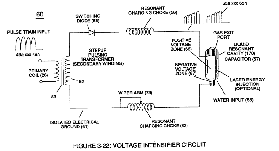
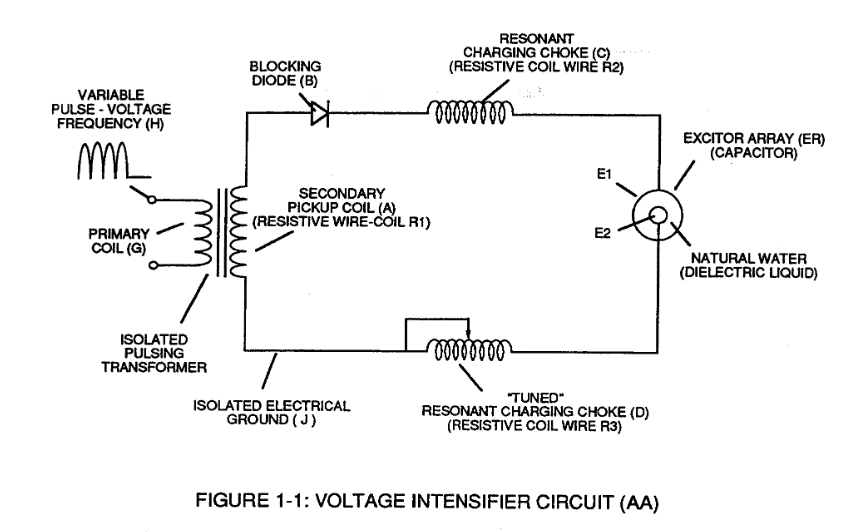
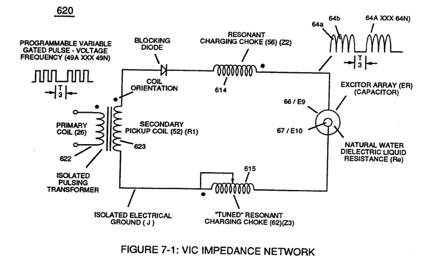
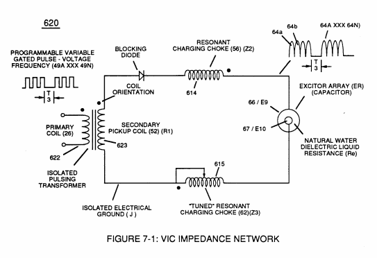
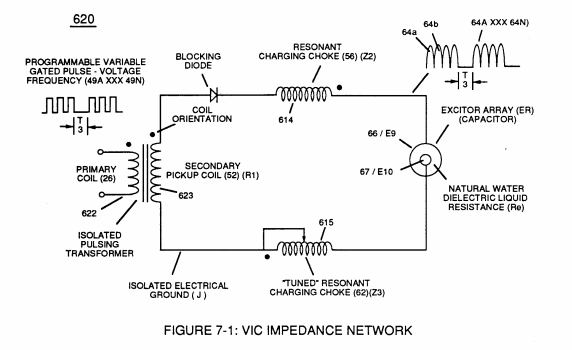
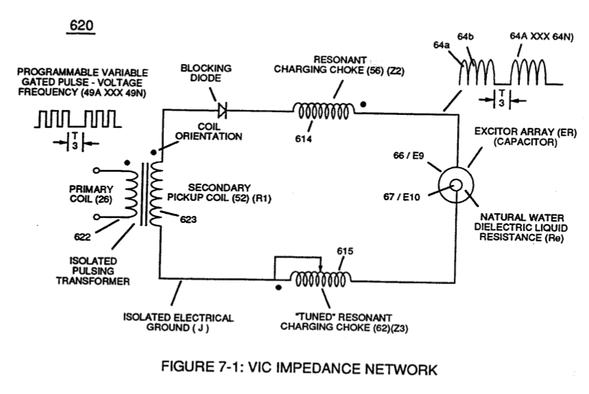
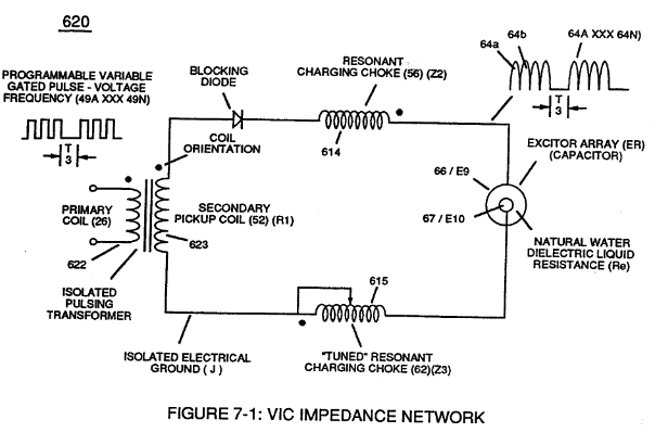
**Voltage Intensifier Circuit** (60) of Figure (3-22) ([Memo WFC 422 DA](https://stanslegacy.com/books/the-birth-of-new-technology/chapter/wfc-422da-wfc-hydrogen-gas-management-system "WFC 422DA - WFC Hydrogen Gas Management System")) as to Figure (1-1) (Memo WFC 420) and **Voltage Intensifier Circuit** (620) of Figure (7-1) are specifically designed to restrict amp flow during **Programmable Pulsing Operations** (49a xxx 49n) but in different operational modes:
| Voltage Intensifier Circuit (60) of Figure (3-22)
[](https://stanslegacy.com/uploads/images/gallery/2023-12/qE3cQ0pxOpRPnR0h-image-1702450549031.png)
| Figure (1-1) (Memo WFC 420)
[](https://stanslegacy.com/uploads/images/gallery/2023-12/nE8xp40ioBIjm8vR-image-1702450578980.png)
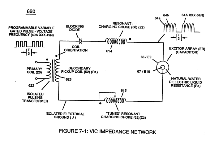
| Voltage Intensifier Circuit (620) of Figure (7-1)
[](https://stanslegacy.com/uploads/images/gallery/2023-12/wKUrbHtXacnQw5dk-image-1702450606619.png)
|
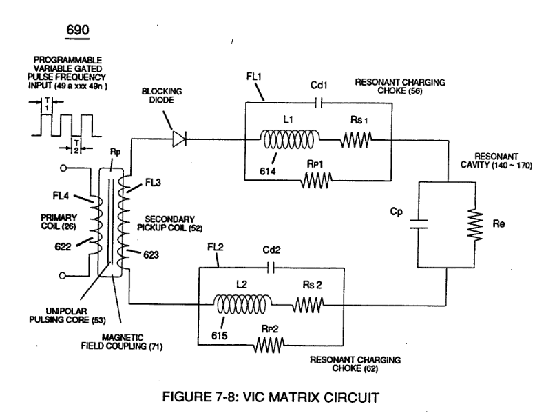
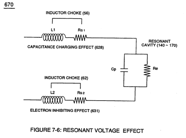
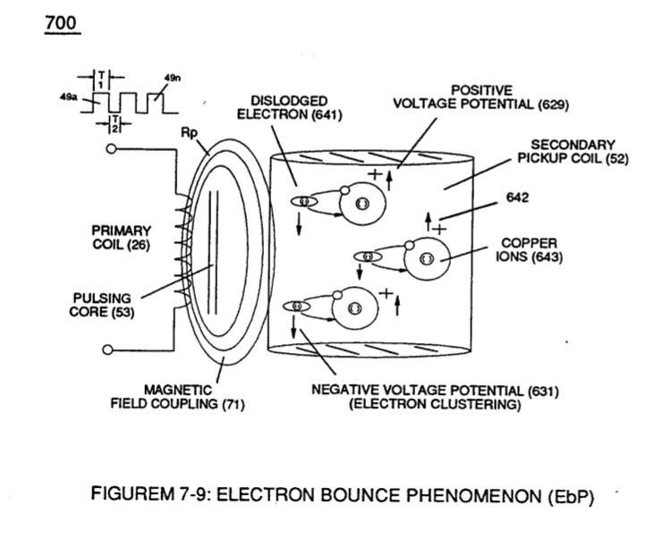
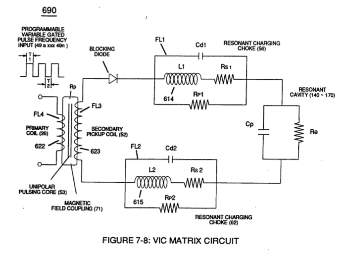
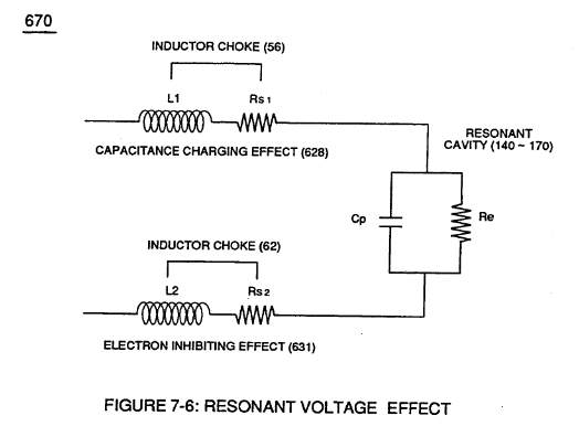
VIC voltage circuit (60) utilizes copper wire-wrap to form **Resonant Charging Chokes** (56/62) of Figure (3-22) in conjunction with **Switching Diode** (55) to encourage and make use of "**Electron Bounce**" phenomena (700) of Figure (7-9) to help promote **Step Charging Effect** (628) of Figure (7-7) by preventing electrical discharge of **Resonant Cavity** (140 - 170) since **Blocking Diode** functions as an "**Open**" switch during **Pulse Off-time**;
whereas,
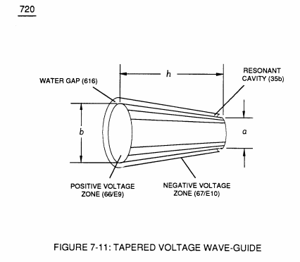
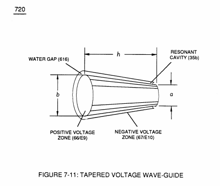
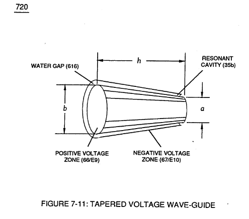
**VIC Voltage Enhancement Circuit** (VIC - VB) (620) of Figure (7-1) incorporates the use of **stainless steel wire-wrap coils** (614/615) to accomplish the formation of unipolar gated pulse-wave (64a xxx T3 xxx 64n) without experiencing "**signal distortion**" or "**signal degradation**" (preventing transformer ringing during signal propagation) as elevated voltage levels ( - xx Vc- xx Vd - xx Vn) while allowing the reduction of **Capacitor-Gap** (Cp) (616) of Figure (7-11) width spacing (57 of Figure 3- 25 ~35 of Figure 6-2) (typically .060 - .010) respectively as illustrated in **Tubular Resonant Cavity** (170) as to **Taper Resonant Cavity (**620) of Figure (7-1).
| (VIC - VB) (620) of Figure (7-1)
[](https://stanslegacy.com/uploads/images/gallery/2023-12/ZEMAYa97rz1qMSUW-image-1702521805142.png)
| (616) of Figure (7-11)
[](https://stanslegacy.com/uploads/images/gallery/2023-12/XgXLgArcunR7Ioqh-image-1702521824943.png)
|
| (57 of Figure 3- 25 ~35 of Figure 6-2)
[](https://stanslegacy.com/uploads/images/gallery/2023-12/S3eCHXNW0INz4ErI-image-1702447512076.png)
| |
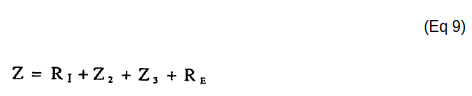
**Switching Diode** (55) of Figure (3-22) prevents Bidirectional electron flow (current flow in one direction only) since **Blocking Diode** (55) only conducts "current flow" in the direction of schematic-arrow while being placed in-line with **VIC Circuit** impedance interaction (R1 + Z2 + Z3 + Re), as mathematically extrapolated in **Circuit Equation** (Eq 9)
... **Diode** (55) being placed between **Secondary Pickup Coil** (52) and **Resonant Charging Choke** (56) to act as an electronic switch in open-position during pulse off-time (**T2**) of Figure (7-8) while preventing electron flow in reverse direction when **Inductor** (L1) **collapsing electromagnetic field** (FL1) produces another **unipolar pulse wave-form** (64a - 64b).
... producing **unipolar voltage wave-form** (64a xxx 64n) during repeated pulse-signal (46a xxx 46n) on-time (T1a xxx T1n)
... allowing the formation of an gated pulse-frequency pulse-train (64a/64b - T3 - 64a/64b) when pulse off-time (T3) is greater than time-period (T2)
... input-signal (49a xxx 49n) being a **Pulse-Train** where (T2) **pulse offtime** (T2) is adjusted to allow **Unipolar Pulse-Train** (64a xxx T3 xxx 64n)
... outputting **Voltage-wave signal** (64a xxx 64n) being a pulse-frequency doubler due to **Inductance Reactance** (FL) of **Inductor Coil** (56) of Figure (3-22) when collapsing magnetic field (FL) of Figure (7-3b) re-cuts **coil-wrap** (Ll) during each pulse off-time (T2)
... producing a second **unipolar voltage wave-form** (64b) during the rise and fall of **magnetic field** (71), as further illustrated in (620) of Figure (7-1)
# Resistance (Rs)
In reference to the use of **stainless steel (s/s) coil-wrap** (614/615), resistive wire value (Rs1/Rs2) of Figure (7-8) (typically 11.6K ohms per coil) is sufficient enough to inhibit current flow oscillation in direct relationship to circuit impedance (Eq. 9) since "current flow" is, also, restricted in the milliampere (s) range due to (s/s) wire material (Rs1/Rs2) composition ability to oppose electron interaction or electron interchange from one atomic structure to another;
while, at the same time, conducting and permitting the transmission of "**Voltage Potential**" across circumference surface area (skin effect) (66/67) of Figure (7-11) as to Figure (590) of Figure (6-2) to bring-on and perform **Voltage Wave-Guide** phenomena (57) of Figure (6-2)
... causing and allowing the applied **Electrical Stress** of opposite voltage polarity (ST-ST' - RU-RU') to trigger **Hydrogen Fracturing Process** (390) of Figure (3-42) in an instant of time
... releasing thermal explosive energy (gtnt) (16) of Figure (4-5) on demand from natural water (85) of Figure (3-26) since the dielectric value (Re) of (Eq.9) of **Water Fuel** (85) is further approximated in **Capacitance Equation** (Eq.22), as illustrated in (650) of Figure (7-4) as to **Tapered Voltage Wave-Guide** (720) of Figure (7-11)
| (Eq.9)
[](https://stanslegacy.com/uploads/images/gallery/2023-12/UbDtR88bFBhus4PS-image-1702446030322.png)
| **Capacitance Equation** (Eq.22)
[](https://stanslegacy.com/uploads/images/gallery/2023-12/7DDADpHgskHekyV1-image-1702445610200.png)
|
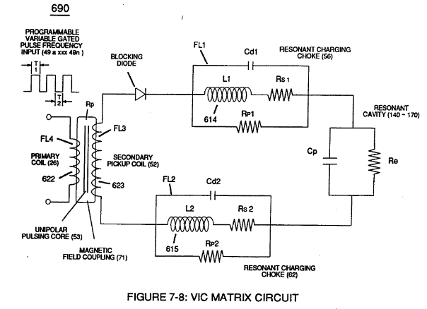
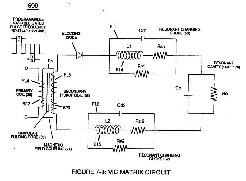
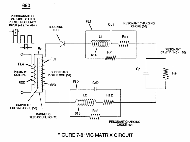
... allowing the dielectric value of **Water** (Re) to be a part of **Voltage Intensifier Circuit** (110) of Figure (4-9) capability of restricting amp flow during **Voltage Pulsing Operation** (49a xxx 49n) of (620) of Figure (7-1) as to **VIC Matrix Circuit** (690) of Figure (7-8)
... allowing applied opposite Voltage potential (ST-ST' - RU-RU') to perform work without amp "influxing", as systematically depicted in VIC Matrix Circuit (690) below.
[](https://stanslegacy.com/uploads/images/gallery/2023-12/8RhgGnTT3BBYWsGx-image-1702447603158.png)
# Inductance (FL)
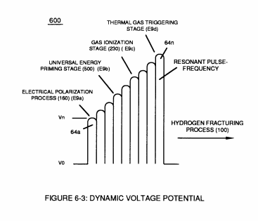
**Component Interaction** promotes **Component Reactance** during D.C. pulsing operations while allowing variable voltage amplitude (Vo - Va -Vb - Vn) of Figure (7-13) to be attenuated independently of **Voltage Pulse frequency** (49a xxx 49n), as so illustrated in (600) of Figure (6-3).
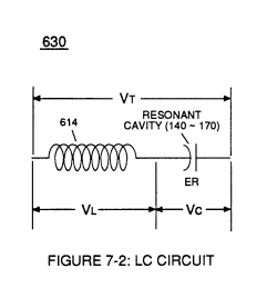
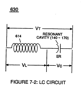
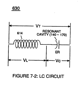
**Resonant Charging Circuit** (630) of Figure (7-2) being an LC Circuit is fanned when **Inductor** (614) of Figure (7-1) is electrically linked to **Taper Capacitor** (720) of Figure (7-11) in series arrangement.
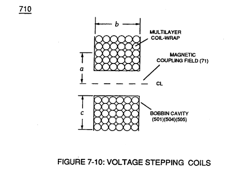
**Inductor** (614) is an insulated wire wound in a spiral pathway around **Bobbin Cavity** (580) of Figure (6-1) to form **Voltage Stepping Coil** (710) of Figure (7-10) as to (580) of Figure (6-1).
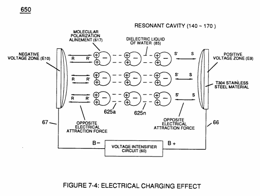
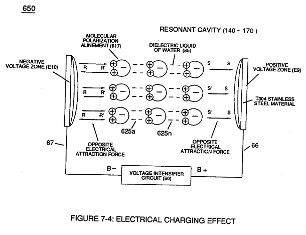
**Capacitor** (E9/E10) of figure (6-2) as to (720) of Figure (7-11) is formed when **outer tapered surface** (66) and **inner tapered surface** (67) forms **Water-Gap** (616) of Figure (7-11) as to Figure (590) of Figure (6-2) having placed there between **Dielectric Water Bath** (85/Re), as schematically illustrated in matrix outline in (670) of Figure (7-6) as to (690) of Figure (7-8) and further detailed in **Electrical Charging Effect** (650) of Figure (7-4).
**Component Reactance** to D.C. pulsing transforms **Inductor** (614) of Figure (7-1) / **Capacitor** (E9/E10) of Figure (7-11) LC circuit of Figure (7-2) into an **Resonant Charging Choke** (614) which steps up an unipolar oscillation of an given charging frequency with the effective capacitance of a **pulse-forming network** (64a xxx 64n) of Figure (7-1) as to (600) of Figure (6-3) in order to charge **Voltage Zones** (E9/E10) to a higher potential beyond applied voltage input
| **Inductor** (614) of Figure (7-1)
[](https://stanslegacy.com/uploads/images/gallery/2023-12/MzvPeyjbCL5eKKdo-image-1702523206210.png)
| **Capacitor** (E9/E10) of Figure (7-11)
[](https://stanslegacy.com/uploads/images/gallery/2023-12/we95r1OtxtgObNm1-image-1702523235713.png)
| LC circuit of Figure (7-2)
[](https://stanslegacy.com/uploads/images/gallery/2023-12/DJ53zhMs2MJCXMU1-image-1702523248932.png)
|
| (600) of Figure (6-3)
[](https://stanslegacy.com/uploads/images/gallery/2023-12/LnZPOrM8WkzklnDw-image-1702523261641.png)
|
|
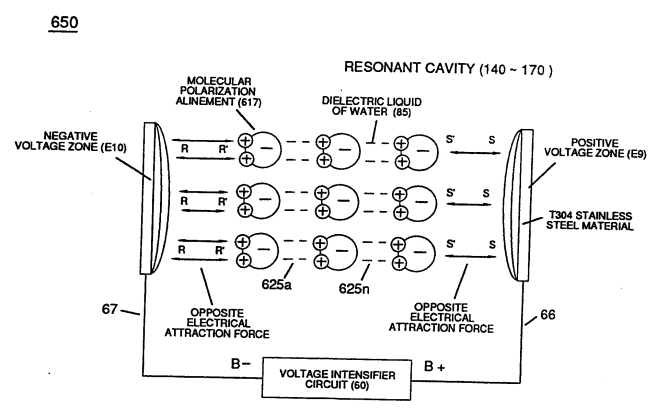
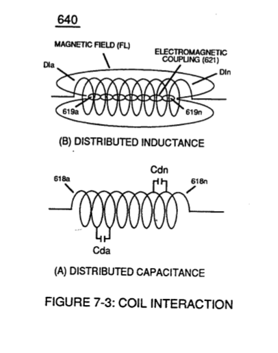
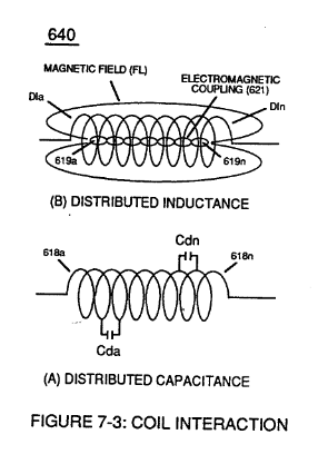
... interacting **Distributed Capacitance** (Cda xxx Cdn) and **Distributed Inductance** (D1a xxx D1n) of Figure (7-3) of **Inductor Coil** (614) of (7-1) with "**Electrical Charging Effect**" brought on by the dielectric value of water bath (85/Re), as pictorially illustrated in (650) of Figure (7-4).
(650) of Figure (7-4)
[](https://stanslegacy.com/uploads/images/gallery/2023-12/SzIwo8acjqHB6coL-image-1702523354217.png)
The established **Dielectric Value of Water** (85) being 78.54 ohms since the electron "L" orbit of the water molecule (210) of Figure (3-27) occupies the maximum allowable number of eight electrons when covalent linkup of 'unlike oxygen atom (76) and hydrogen atoms (77a/b) occurs' stabilizing **Water** molecule (85) into existence ... thereby, maintaining molecular stability of water by opposing the exchange of electrons from an external electron source (amp inducing circuit) beyond molecular Structure (85).
Electron interaction (movement of electrons through the liquid medium of water) is further inhibited since natural water contaminates (144a xxx 144n) of Figure (3-24) is normally less than 20 ppm.
Figure (3-24)
[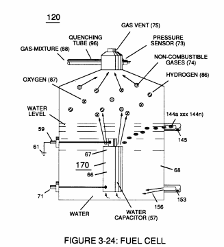](https://stanslegacy.com/uploads/images/gallery/2023-12/Kfu24EK7tggNsqf0-image-1702523475722.png)
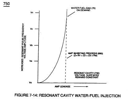
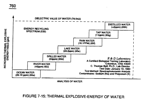
... distilled water, of course, is generally lab-tested 1ppm or less, as illustrated in (760) of Figure (7-15) as to (750) of Figure (7-14).
# Capacitance (Cd)
**Capacitor** (E9/E10) of Figure (7-1) as to Figure (650) of Figure (7-4) in direct relationship to **Water Gap** (616) becomes **Taper Resonant Cavity** (720) of Figure (7-11) as shown in (590) of Figure (6-2) since **Water Gap** (616) is occupied by a dielectric liquid (Re) as herein before identified as **natural water** (85) having no electrolyte added thereto
... generally **rain water** (85f) (750) of Figure (7-14) being almost free of contaminates due to **Water Evaporation Process** (532) of Figure (5-6) ... **rain water** (850 being an **liquid-insulator** that restricts the flow of amps
... a resistive liquid (*having an ohmic value of 78.54 ohms*) that takes on an "**Electrical Charge**" when **applied voltage Potential** (66/67) of Figure (7-1) as to (650) of Figure (7-4) causes and sets up **Molecular Polarization Alignment** (617) of Figure (7-4) by way of **electrical molecular rotation** (*opposite electrical attraction force to rotate and position particle alignment*) of each **water Molecule** (85a - 85b - 85c - 85n). being subjected to **opposite electrical attraction forces** (SS' - RR').
In like manner, the stainless steel (s/s) T304 material that forms **Voltage Zones** (E9/EI0) undergo **particle alignment** of its **atomic structure** within the atomic infrastructure of plate-material (E9/E10) when exposed to the same applied electrical voltage fields (66/67) after a pre-set time
... causing **molecular electrical movement** to occur within the surface-material (E9/EI0)
... which, after occurring, the newly formed **molecular electrical orientation** (625a xxx 625n) of Figure (7-4) remains in electrical atomic alignment after pulse off-time (T2) aiding the transference of voltage potential during pulse on-time (T1)
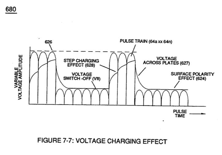
.. allowing the resultant **Surface Polarity Effect** (skin effect) (624) of Figure (7-7) to supply a sufficient residual atomic "**Electrical Charge Field**" to help maintain molecular alignment of water atoms (617) during pulsing operations, as illustrated in (680) of Figure (7-7).
Inherently, then, **Resonant Cavity** (720) of Figure (7-11) as to (650) of Figure (7-4) forms **capacitor** (ER) of Figure (7-1) when the dielectric liquid of **water** (85) is placed or injected between **electrical conducting plates** (E9/E10) while **applied voltage Potential of opposite polarity** (66/67) is directly exposed to **Water Molecules** (85a xxx 85n), as depicted in **Taper Resonant Cavity** (590) of Figure (6-2) as to (650) of Figure (7-4).
**Inductor** (614) and **Inductor** (615) of Figure (7-1) as to (670) of Figure (7-6) is wound or coil-wrapped (*see multi-layer equation Eq. 20*) in such a manner as to increase the **magnetic flux intensity** (D1a xxx D1n) of Figure (7-3) as to (580) as to Figure (6-1) in reference to (710) of Figure (7-10) between the **turns** (618a xxx 618n) of **coil-wrap** (640).
The circular-spiral turns of wire (forming parallel electrical surfaces) is separated by an **Insulated Dielectric Coating Material** which forms a series of capacitors (Cda xxx Cdn) when magnetic flux-lines (619a xxx 619n) produce **Electromagnetic Coupling Field** (621) during pulse on-time (T1), as illustrated in (640) of Figure (7-3) as to (690) of Figure (7-8).
The **series resistance value** (Rs) in (670) of Figure (7-6) as to (690) of Figure (7-8) and (670) of Figure (7-6) is determined by the composition of the wire material in terms of its **ohmic value** (electrical resistivity) per given length and diameter cross-section:
**Resonant Charging Chokes** (614/615) 430F/FR 36 AWG (.006) stainless steel (s/s) wire equals **60 micro ohms per centimeter**;
**Primary Coil** (622) 22 AWG (.028) copper wire equals 5.1933 ohms per pound weight;
**Secondary Pickup Coil** (623) 35 AWG (.007) copper wire equals 13K ohms per pound weight.
"**Pyre-ML**" trade name "**Himol**" polymer coating-material is used to impart thermal and mechanical resistance to the stainless steel (s/s) wire (614/615) coating; both magnet wire sizes (622/623) uses solderable **Nysol** (Polyurethane Nylon Jacket) insulation enamel coating as a electrical shield-material
... all dielectric coatings having an effective 3KV per mil dielectric value and formulated specifically to endure automotive temperature range from -40 C to 155 C.
# Inductance Reactance (Rs - Cd - FL)
**Inductance Reactance** occurs when resistance (Rs), capacitance (Cd), and Inductance (FL) interacts together during D.C. Pulsing (49a xxx 49n), as schematically depicted in (690) of Figure (7-8).
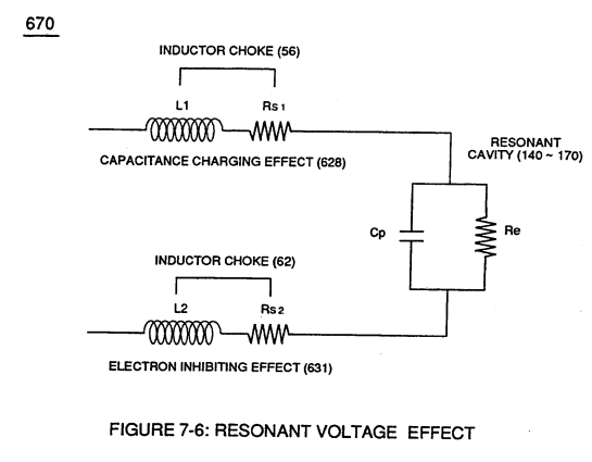
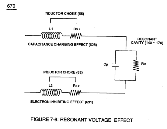
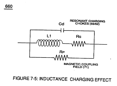
**Inductance Reactance** not only increases voltage across water-capacitor (ER) beyond applied **Voltage Potential** (626) of Figure (7-7) but, also, establishes "**Impedance Field**" (FL) across **Inductors** (L1-L2) of Figure (7-6) which acts and performs as **Resonant Charging Chokes** (614/615) of Figure (7-1) once placed on opposite side of capacitor (ER) forming **Resonant voltage Effect Circuit** (670) of Figure (7-6), as illustrated in (620) of Figure (7-1) as to (690) of Figure (7-8).
| **Voltage Potential** (626) of Figure (7-7)
[](https://stanslegacy.com/uploads/images/gallery/2023-12/DxHHdQOGcn8xreEZ-image-1702618704743-38-22.png)
| **Inductors** (L1-L2) of Figure (7-6)
[](https://stanslegacy.com/uploads/images/gallery/2023-12/rpg6jPD7jlYgCwQs-image-1702618749219-39-07.png)
|
| **Resonant Charging Chokes** (614/615) of Figure (7-1)
[](https://stanslegacy.com/uploads/images/gallery/2023-12/cGPbFx0DAuoueBNO-image-1702618762437-39-19.png)
| (670) of Figure (7-6)
[](https://stanslegacy.com/uploads/images/gallery/2023-12/HSAV63t6lHwoHa23-image-1702618781512-39-39.png)
|
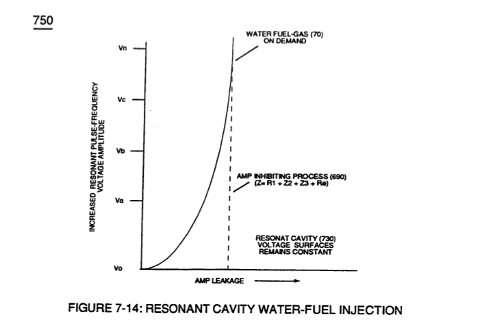
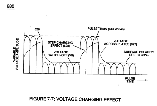
[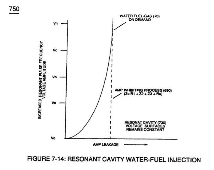](https://stanslegacy.com/uploads/images/gallery/2023-12/QIGKuhIZN7cxFl2A-image-1702618601495-36-35.png)Both Inductors (LI/L2) are Bifilar wound in equal length to **optimize the electromagnetic field strength** (FL) in equal electromagnetic intensity (FL1 = FL2) to encourage and promote "**Electron Bounce**" phenomenon (700) of Figure (7-9) while adjusting (programmable pulse wave-form) input signal **Pulse-Frequency** (49a xx 49n) to "tune-in" to the "dielectric property" (Re) of water (85) causing amp flow to be reduce to a minimum value while allowing voltage potential (627) of Figure (7-7) to go toward infinity if the electronic components would allow it to happen, as graphically illustrated in (750) of Figure (7-14).
| "**Electron Bounce**" phenomenon (700) of Figure (7-9)
[](https://stanslegacy.com/uploads/images/gallery/2023-12/09D7i86bQoPuSMok-image-1702618687969-38-05.png)
| (627) of Figure (7-7)
[](https://stanslegacy.com/uploads/images/gallery/2023-12/DxHHdQOGcn8xreEZ-image-1702618704743-38-22.png)
|
**Inductance Field** (L1-FL1) performs "**Capacitance Charging Effect**" (628);
while, at the same time, **Inductor Field** (L2-FL2) restricts electron movement through **VIC Impedance Network Circuit** (620) of Figure (7-1) since **Inductance Field** (FL2) locks onto **Electrons Magnetic Field** (547) of Figure (5-9) to block the movement of electron flow toward **Positive Voltage Potential** (66)
... thereby preventing and inhibiting electron-flow to pass through or arc-over capacitor water-gap (Cp) of Figure (7-8) such electron blocking action is herein called "**Electron Inhibiting Effect**" (631), as denoted in (670) of Figure (7-6) as to (750) of Figure (7-14).
At elevated or higher amplitude voltage levels (xxx Ve xxx Vf xxx Vn), **primary electromagnetic coupling field** (Rp) of Figure (7-8) transmitted by way of **Inductance Pulsing-Core** (190) of Figure (3-23) as to **VIC Coil Assembly** (580) of Figure (6-1) enters into and passes through both Inductors (L1/L2) simultaneously and offers not only further electron-flow restriction (Rp1/Rp2) to both **Inductor Chokes** (56/62) but automatically increases voltage potential (xxx V g xxx Vh xxx Vn) of opposite voltage intensity of equal magnitude (66/67) across **Resonant Cavity** (140 -170)
... overcoming any potential loss of pulse signal due to resistive interaction (Rsl/Rs2) of either or both **Inductor Cores** (L1/L2) wire-material to the formation of **Inductance Fields** (FL1/FL2) during reoccurring pulse on-time (T1a xxx T1n).
**Electron Inhibiting Effect** (631) in direct relationship to **Voltage Enhancement Effect** (528) is accomplished since stainless steel 430F/FR wire-material is "**Electromagnetic Inductive**" to incoming electromagnetic flux-lines (71a xxx 71n) (Rp) without (s/s) inductor-wire-coil (L1/L2) becoming permanently magnetized
... paralleling and performing the same electromagnetic characteristic of copper wire when it comes to magnetic field reformation (Rp - Rp 1 - Rp2) of Figure (7-8), as further illustrated in electromagnetic coupling fields (71 - 511 - 512) of Figure (6-1) that encourages, brings-on, and perform **Voltage Inducement Process** (580) of Figure (6-1) as to (620) of Figure (7-1) without amp "influxing" (inhibiting amp flow) between **Positive Voltage Potential** (66) and **Negative Voltage Potential** (67) electrically applied across **Resonant Cavities** (140 -170).
(620) of Figure (7-1)
[](https://stanslegacy.com/uploads/images/gallery/2023-12/cGPbFx0DAuoueBNO-image-1702618762437-39-19.png)
# In-Line Circuit Components
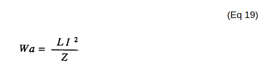
**Lengthening Inductor** (L1/L2) lengths applies an even higher **Voltage Potential** (66/67) across **Resonant Capacitor** (140 -170) (ER) since **Inductance Reactance** "Stores" Energy and, is expressed by:
[](https://stanslegacy.com/uploads/images/gallery/2023-12/PGspwajDDA6KDyzJ-image-1702450266766.png)
Where,
(Wa) is the energy in **Joules** (**Watt-seconds**); (L) is the **Inductance** in **Henries**; and (I) is the **current** in **amperes**.
**Inductance Reactance** directly determines "**Stored**" Energy (Wa) which is controlled by input **Voltage Potential** attenuated or varied by way of **Voltage Amplitude** (Vo xxx Va xxx V b - Vf xxx Vg xxx Vn) of Figure (7-13) and/or **Gated Pulse-Frequency** (49a xxx 49n - T3 - 49a xxx 49n), or both.
**Inductance Reactance** performs several functions simultaneously or to given stimuli:
- increases applied voltage amplitude (Vo - Vn)
- doubles input frequency (64a \* 64b) when 50% Duty Cycle Pulse (T1 = T2) is inputted
- effectuates "Step Charging Effect" (680) of Figure (7-7) when Pulse off-time (T2) is less than Pulse on-time (T1)
... determining **voltage swing** from **highest voltage level** (Vn) to **volts switch-off point** (Vff), and establishing **Impedance** (FL) which minimizes heat loss of electrical input power (49) by impairing electron movement.
**Inductor** (Ll) acts and performs in like manner to **Inductor** (L2) since both **Inductor** (L1/L2) are physically the same size and shape.
**Thermal Explosive Energy-Yield** (gtnt) (16a xxx 16n) instantly produced from water (85) is determined by:
- **Voltage Amplitude** ( xxx Vn)
- **Duty Cycle of Pulse Train** (T1 - T2a xxx T1 – T2n)
- **Gated Pulse-Frequency** of applied **Voltage Potential** (49a xxxx 49n - T3 - 49a xxx 49n)
- **Inductor** (L1/L2) length
- **Secondary Pickup Coil** (523) Length (FL3a xxx FL3n)
- dielectric gap-spacing (Cp)
- or any combination thereof.
# Multi-layer Coil
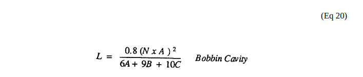
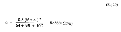
**Inductance** of a multi-layer coil of rectangular cross section can be computed by below formula when optimizing maximum distributed capacitance (Cda xxx Coo) and distributed inductance (Dla xxx Dln) of Figure (7-3) to intensify **Inductance Field Strength** (FLa xxx FLn) to function as a voltage multiplier in switch-off conditions (612a xxx 612n), as illustrated in (710) of ~ . Figure (7-10) as to **VIC Coil Assembly** (580) of Figure (6-1) and, is expressed:
[](https://stanslegacy.com/uploads/images/gallery/2023-12/25qf8F5eQmFzf5CS-image-1702445551138.png)
**Where**,
(L) is the **inductance** in microhenries,
(N) is the **number of** **turns**,
(A) is the **mean radius** in inches,
(B) is the **length of the coil** in inches,
(C) is the **depth of the coil** in inches.
# Taper Resonant Capacitor (ERt)
**Capacitor** (ER) is automatically formed when dielectric liquid of water (Re) is placed between **Electrical Conducting Plates** (E1/E2) of Figure (1-1) page (1-13) ([Memo WFC 420](https://stanslegacy.com/books/the-birth-of-new-technology/chapter/wfc-420-hydrogen-fracturing-process "WFC 420 - Hydrogen Fracturing Process")).
Stainless steel T304 material is used to form **Electrical Voltage-Plates** (EIIE2) which do "not" chemically interact (chemically inert) (Lab tested less than .0001/year decomposition rate) with liberated water gases (hydrogen \_86, oxygen \_87, and non-combustible gases W being exposed to an high intensity voltage pulse-field (64a xxx 64n) with negligible amp flow.
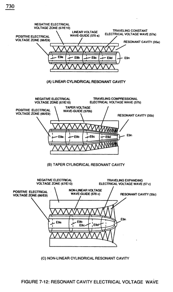
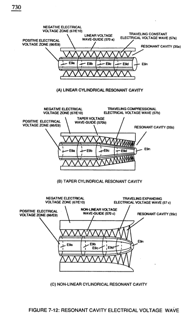
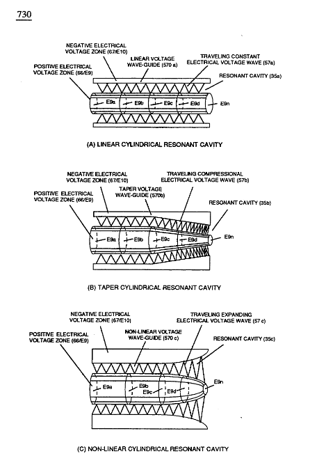
**Electrical Plates** herein called "**Excitor**" Plates or **Voltage Zones** (E1/E2) can take-on different configuration of shapes to maximize **Dynamic Voltage Potential** (600) of Figure (6-3) for different application of usage:
(35a) **Traveling Constant Electrical Voltage Wave** by way of linear cylindrical resonant cavity (Tubular Cavity 730A),
(35b) **Traveling Compressional** (concentrating electrical intensity) **Electrical Voltage Wave** by way of taper cylindrical resonant cavity (730B),
(35c) **Traveling Expanding Electrical Voltage** wave by way of non-linear cylindrical resonant cavity (730C)
... or any voltage surface combination thereof
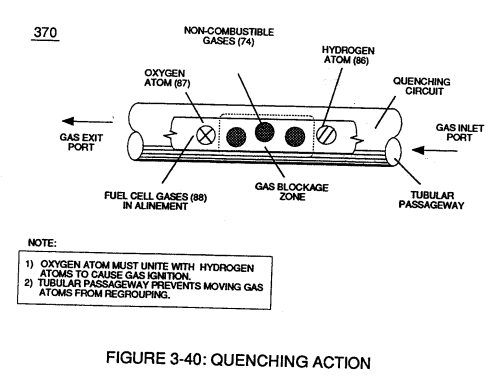
... each resonant cavity design acting and functioning as a **Voltage Wave-guide** (570) and gap-size (35) sufficient enough to allow the "**Quenching Effect**" to take place, as illustrated in (730) of Figure (7-12) as to (370) of Figure (3-40).
| (730) of Figure (7-12)
[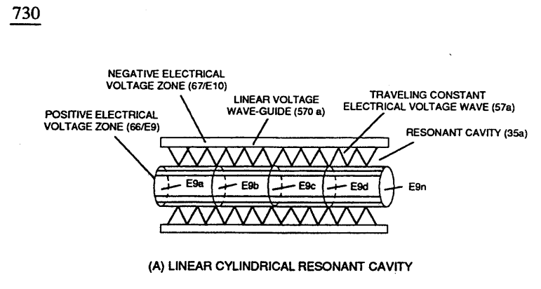](https://stanslegacy.com/uploads/images/gallery/2023-12/ZPYUzojeavXnoKig-image-1702612413679.png)
| (370) of Figure (3-40)
[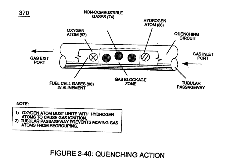](https://stanslegacy.com/uploads/images/gallery/2023-12/8G6ENOaauv9BUBR9-image-1702612439452.png)
|
The dielectric property of water (being 78.54 ohms @ 25° C) permits the storage of '"**Electrical Charge**" when a potential voltage difference exists between **Electrical Voltage-Plates** (E1/E2) as to (E9/E10).
**[](https://stanslegacy.com/uploads/images/gallery/2023-12/FWz40QLyPOJwJefG-image-1702595701485.png)**
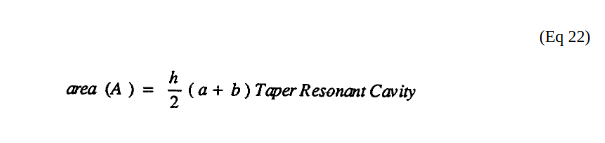
**Capacitance** (Cp) of Figure (7-6) as to (690) of Figure (7-8) is determined by the surface area (A) of **Electrical Voltage-Plates** (E1/E2 - E9/E10), the distance (d) between the **Electrical Plates** (in inches), and the **permittivity** (Eo) of the dielectric property of water (85) and, is expressed in the following equation:
**Where**,
(Eo) is **Free-Space Permittivity of Water** established by **VIC Circuit** (690) of Figure (7-8) ability to restrict amp flow,
(e/Eo) Ratio is the **Dielectric Constant of Water**,
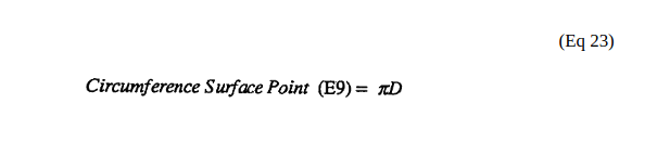
(A) is the surface Area of **Resonant Cavity** and, is expressed in the below equation:
[](https://stanslegacy.com/uploads/images/gallery/2023-12/7DDADpHgskHekyV1-image-1702445610200.png)
**Where**,
(h) is longitudinal length of tapered resonant cavity,
(a) being exit pan circumference surface point (E9d) of Figure (6-2),
(b) being cylindrical circumference surface point (E9a) of Figure (6-2) where tapered surface starts,
(a) (b) circumference surface points (E9a)(E9d) respectively determined by below expressed equation:
(see diagram 720 of Figure 7-11)
[](https://stanslegacy.com/uploads/images/gallery/2023-12/nGqEpPvBXerFXvQV-image-1702445834337.png)
**Where,**
(D) is diameter cross section of cylindrical surface at designated point (E9a - E9n),
(x) being mathematical constant 3.1416.
| diagram 720 of Figure 7-11
[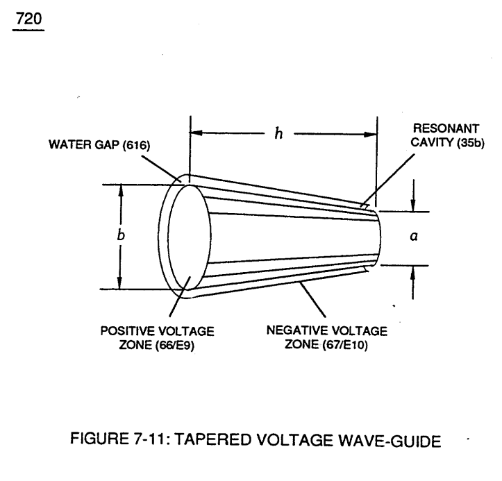](https://stanslegacy.com/uploads/images/gallery/2023-12/nZspZRIZeJzET3th-image-1702612195058.png)
|
# Capacitance Reactance
**Capacitance Reactance** is determined by the insulation resistance (Rs+Re) and **Inductance** (L1/L2) interacting together during D.C. Pulsing.
Dielectric property of water opposes amp leakage (Re) while another property of water takes-on an "**Electrical Charge**".
Water temperature (Rt) (cool-to-the-touch) keeps (Re) constant since amp flow remains minimal.
**Plate Inductance** (Lc) is **Inductance Reactance** of **Inductor** (L1 ) and **Inductance Reactance** of **Inductor** (L2) in series with **Resonant Capacitor** (140 -170) of Figure (7-6) as to (690) of Figure (7-8).
| **Resonant Capacitor** (140 -170) of Figure (7-6)
[](https://stanslegacy.com/uploads/images/gallery/2023-12/9aPfvETrheVTgOak-image-1702613092794.png)
| (690) of Figure (7-8)
[](https://stanslegacy.com/uploads/images/gallery/2023-12/gzGVEsezx0gmvk9h-image-1702612335114.png)
|
In terms of **Component Reactance**, Inductors (L1/L2) should always be larger than **Capacitor** (ER) of Figure (7-2) in order to maximize amp restriction to enhance "**Voltage Deflection**" (SS' - 617a xxx 617n - RR') of Figure (7-4) and, is expressed by :
| **Capacitor** (ER) of Figure (7-2)
[](https://stanslegacy.com/uploads/images/gallery/2023-12/ld2UDKOKxvKptiGw-image-1702613172661.png)
| "**Voltage Deflection**" of Figure (7-4)
[](https://stanslegacy.com/uploads/images/gallery/2023-12/Dk0i0rZslFjtQ0mh-image-1702613196411.png)
|
[](https://stanslegacy.com/uploads/images/gallery/2023-12/APaEvYdBZl9k2Iyy-image-1702445998069.png)
**Whereas**,
**Capacitor** (ER) should remain relatively small due to the dielectric value of water to obtain maximum **Thermal Explosive Energy-Yield** (16a xxx 16n) of Figure (4-5) and subsequently establishing **Quenching Circuit** (370) of Figure (3-40) to prevent gas ignition inside traveling voltage wave-guide (590) of Figure (6-2) as to (730) of Figure (7-12)
| **Quenching Circuit** (370) of Figure (3-40)
[](https://stanslegacy.com/uploads/images/gallery/2023-12/6YdTq2g8mdXowsG1-image-1702612910404.png)
| (590) of Figure (6-2)
[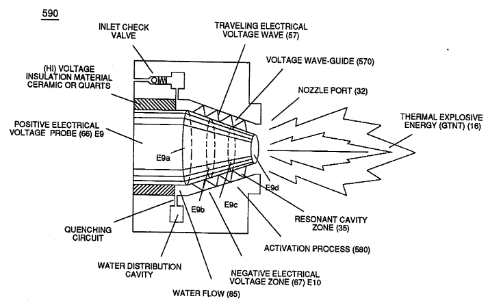](https://stanslegacy.com/uploads/images/gallery/2023-12/yfkyykTD8kyZ0ZlP-image-1702321431762.png)
| (730) of Figure (7-12)
[](https://stanslegacy.com/uploads/images/gallery/2023-12/ZPYUzojeavXnoKig-image-1702612413679.png)
|
... to bring-on and trigger Hydrogen Fracturing Process (390) of Figure (3-42) once liberated and expanding water gases (100) of Figure (4-8) passes beyond exit port (E9d)
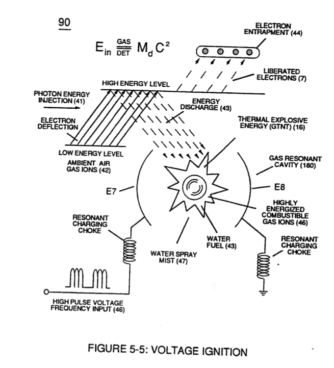
... activating Voltage Ignition Process (90) of Figure (5-5)
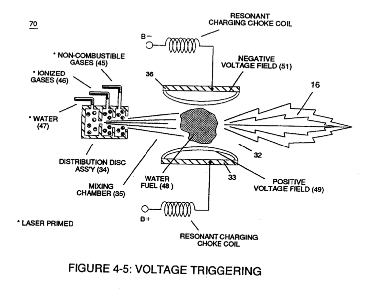
... utilizing **Dynamic Voltage Potential** (600) of Figure (6-3) of opposite electrical stress (SS' - 617 - RR') to cause **thermal atomic agitation** (90) of Figure (4-7) (kinetic heat by atomic motion)
which, when occurring at **gas exit port** (32) of Figure (4-5), spark-ignites expanding water gas-fuel (45/46/47) of Figure (4-5) during water inject cycle (70) of Figure (4-5)
... releasing thermal explosive energy (gtnt) (16) under control state.
# Circuit Resistance
Total VIC "**Circuit Resistance**" to D.C. current flow is expressed and determined by:
[](https://stanslegacy.com/uploads/images/gallery/2023-12/UbDtR88bFBhus4PS-image-1702446030322.png)
**Where**,
(Rl) is the resistive value of **Secondary Pickup Coil** (52) of Figure (7-8) plus **Magnetic Field** strength of **primary coupling field** (71) in direct relationship to **inductance field strength** (Rp) which is determined by the number of turns of wire that make up secondary coil-wrap (52),
(Z2) is determined by inductance field strength (FL1) and resistive value (RS1) (typically 11.6 KQ) of stainless steel (s/s) wire-coil (56) (LI) when being exposed to external magnetic coupling field strength (Rp),
(Z3) is determined by **inductance field strength** (FL2) and **resistive value** (RS2) (typically 11.6KQ) of stainless steel (sls) wire-coil (62) (L2) when being exposed to the same external **magnetic coupling field strength** (Rp)
... each choke-coil (LIIL2) being of the same impedance value since both coil-wraps (56/62) are Bifilar wound together onto a single **spool-bobbin**, (Re) is the dielectric property of water and it's resistive value is typically (78.54 Q) since "**rain water**" (85f) contains less than 20ppm of any type of contaminates due to **Water Evaporation Process** (530) of Figure (5-6).
see **VIC Matrix Circuit** 690 of Figure 7-8 as to **Water Chan** (760) of Figure (7-15), once again
# Transformer Action
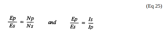
**Inductance Core** (53) of Figure (6-1) composed of "**Grain Oriented**" Electrical Steel laminations step up applied **Voltage** (49) when **Magnetic Field Coupling** (71) of Figure (7-8) cross over to **Secondary Pickup Coil**-winding (52) which has more turns of wire than **Primary Coil-** winding (26) by way of "**Eddy**" currents that induce magnetic flux lines of forces (71a xxx 71n) emanating away from magnetic core material (53) and caused by **Primary Coil** (26) being electrically energized during pulsing operations (T1a xx T1n), as illustrated in (690) of Figure (7-8).
**Magnetic Induction** (71a - 71n) is determined by **Inductance Permeability** (μL) of core material (53) along with VIC circuit geometry ability to step up **Voltage Potential** (Vo - Vn) by way of "**Transformer Action**", and is expressed in the following equations:
[](https://stanslegacy.com/uploads/images/gallery/2023-12/XSHM5TpNJbvKWdwg-image-1702446091555.png)
**Where**,
[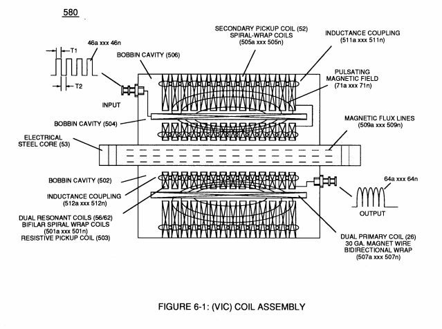](https://stanslegacy.com/uploads/images/gallery/2023-12/nQymCnRuuu9kwxZK-image-1702523026667.png)(Ep) is voltage induced in Primary Coil (26),
(Es) is Voltage induced in Secondary Coil (52),
(Np) is the number of turns of wire that make up **Primary Coil-Wrap** (504) of Figure (6-1),
(Ns) is the **number of turns** of wire that make up **Secondary Coil-Wrap** (505) of Figure (6-1),
(Is) is the established current flow (**under load**) in **Secondary Coil-Winding** (52) ,
(Ip) is the amount of current flow in the **Primary Coil-Winding** (26) when electrically "energized" during pulsing operations (49a xxx 49n - T3 - 49a xxx 49a).
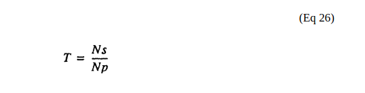
The turns ratio of the **VIC Transformer** (26/52) is determined by the following equation:
[](https://stanslegacy.com/uploads/images/gallery/2023-12/0FfSa2XjWgyWvDtp-image-1702446102303.png)
**Where**,
(Ns) is the number of turns of wire for each bobbin cavity (505) of Figure (6-1) as to (710) of Figure (7-10) that are electrically connected in series arrangement (505a xxx 505n) to form **Secondary** **Coil-Wrap** (52),
(Np) is the number of turns of the **Primary Coil** (26) wire-wrapped about spool cavity (504)
[](https://stanslegacy.com/uploads/images/gallery/2023-12/lQrzUXSnbY5rtQb2-image-1702595344873.png)... each bobbin cavity adhering to equation (Eq 20), as illustrated in (710) of Figure (7-10).
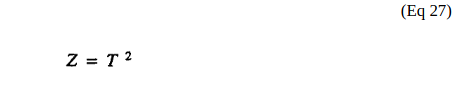
The **impedance ratio** of VIC transformer is determined by:
[](https://stanslegacy.com/uploads/images/gallery/2023-12/d2LspWrLSsIZZ8i0-image-1702446118191.png)
**Where**,
(1'2) is the sum of the magnetic field strength (FL4) of the **primary coil** (26) and the **induced magnetic field** (FL3) of the **Secondary Pickup Coil** (52) during each pulse cycle (T1) in direct relationship to repetitive pulse cycling (T1a xxx T1n) and both magnetic fields (FL3/FL4) interacting, and is expressed in the following equation:
[](https://stanslegacy.com/uploads/images/gallery/2023-12/2BG3s0gDGp33Yygq-image-1702446130639.png)
**Where**,
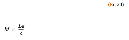
(M) is the mutual inductance expressed in the same units .as (La),
(La) is the total inductance of **Primary coil** (26) and Secondary coil (52) with fields aiding **Coupling Inductance** (Rp) between the **Primary coil** (26) and **Secondary Coil** (52) is further extrapolated in the following equation:
[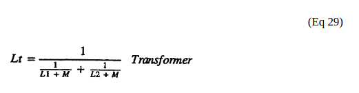](https://stanslegacy.com/uploads/images/gallery/2023-12/cT0wusDcHXsvGdp5-image-1702446153461.png)
**Where**,
(Lt) is the total inductance,
(L1) and L2) are the inductances of each individual transformer coils (26)(52),
(M) is the mutual inductance of each transformer coil (26/52) being in parallel relationship with fields aiding **Coupling Inductance** (Rp1) and (Rp2) in (690) of Figure (7-8) is further expressed in the following equation:
[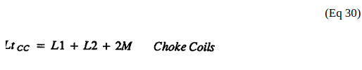](https://stanslegacy.com/uploads/images/gallery/2023-12/Eyi5pwuUvYxixdvm-image-1702446178855.png)
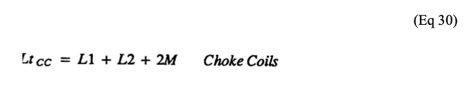
**Where**,
(Lt cc) is the total inductance of **Choke Coils** (FL1 - FL2),
(L1) and (L2) are the inductances of each individual choke coil (56)(62) in series with **Secondary Coil** (52) **Electrical Voltage**
**Potential** (700) of Figure (7-9) and being exposed to the same **Voltage Transformer** (26 - 53 - 52) magnetic field (Rp) with aiding fields,
(M) is the mutual inductance of choke coils (L1/L2) since **Transformer Magnetic Field** (Rp) is the excitation **External Magnetic Field** (Rp1/Rp2) by way of **Unipolar Pulsing Core** (53).
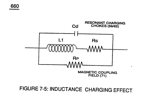
**VIC Coil Assembly** (580) of Figure (6-1) as to (690) of Figure (7-8) in reference to **Schematic Circuit** (620) of Figure (7-1) is constructed in such a way as to rotate and position **Inductor Coils** (26 - 52 - 56 - 62) to be of the same electromagnetic polarity orientation, indicator mark (e)
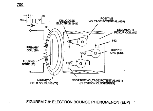
... thus, allowing **Inductance Fields** (FL1 - FL2 - FL3 - FL4) to be aiding one another during the same sequence of pulse-time (T1) ... thereby, allowing **Inductance Charging Effect** (660) of Figure (7-5) and **Resonant Voltage Effect** (670) of Figure (7-6) to interact with the dielectric properties of water (Re) to cause and inhibit electron flow (IF) since "electrons" magnetic field (547) of Figure (5-9) locks onto the electromagnetic fields of each energized choke coils (FL1/FL2) during **Voltage Excitation** (Vo -Vn) which, now, brings on and allows "**Electron Bounce Phenomenon**" (700) of Figure (7-9) to take place.
| **Inductance Charging Effect** (660) of Figure (7-5)
[](https://stanslegacy.com/uploads/images/gallery/2023-12/OJ4oQWHq5REb8uVE-image-1702595636154.png)
| **Resonant Voltage Effect** (670) of Figure (7-6)
[](https://stanslegacy.com/uploads/images/gallery/2023-12/F8SiHklu1rTCr0kf-image-1702595646541.png)
|
| (547) of Figure (5-9)
[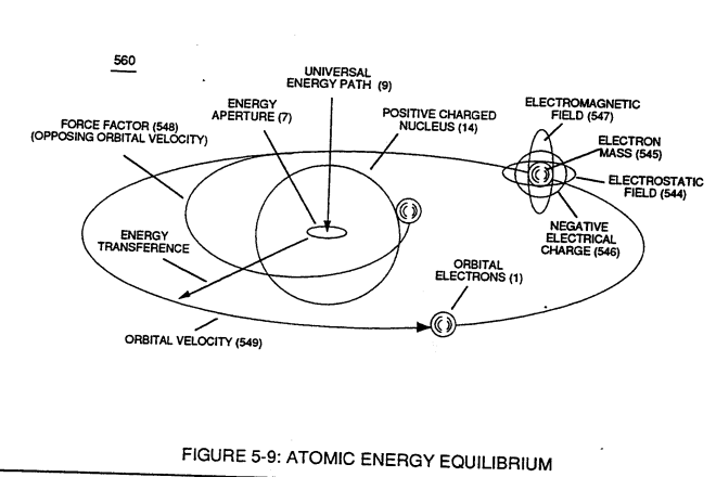](https://stanslegacy.com/uploads/images/gallery/2023-12/VTmtI7b0eETTHgBj-image-1702595664580.png)
| **(700) of Figure (7-9)**
[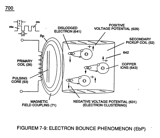](https://stanslegacy.com/uploads/images/gallery/2023-12/SIOmTh50yR29ICJg-image-1702595681532.png)
|
(See Appendix B Note 1)
> **Note 1**) The **Electron Inhibiting Effect** (631) of Figure (7-6) to cause "**Electron Clustering**" (Grouping/collecting negative charged particles at a given point) (700) of Figure (7-9) to produce ''**Negative Voltage Potential**" ( B- ) at one side of **Water Gap** (Cp) of Figure (7-8) is accomplished by low electrical power input (Tab 38) when **Choke-Coil** (62) of Figure (7-1) magnetic field (FL2) (690) of Figure (7-8) during pulse on-time (49) impede "**Electron-Flow**" since electron mass is composed of electromagnetic matter which interacts with magnetic field strength (FL2).
>
> **Capacitance Charging Effect** (628) prevents amp influxing away from **Water Gap** (Cp) in a similar manner
>
> ... producing "**Electrical Stress**" (SS' - RR') (B+/B-) across **Water Gap** (Cp) since *both* **Choke-Coils** (56/62) conduct voltage potential (*Negative or Positive*) during pulsing operations.
| **Electron Inhibiting Effect** (631) of Figure (7-6)
[](https://stanslegacy.com/uploads/images/gallery/2023-12/FWz40QLyPOJwJefG-image-1702595701485.png)
| "**Electron Clustering**" (Grouping/collecting negative charged particles at a given point) (700) of Figure (7-9)
[](https://stanslegacy.com/uploads/images/gallery/2023-12/SIOmTh50yR29ICJg-image-1702595681532.png)
|
| **''Negative Voltage Potential"** ( B- ) at one side of Water Gap (Cp) of Figure (7-8) & magnetic field (FL2) (690) of Figure (7-8)
[](https://stanslegacy.com/uploads/images/gallery/2023-12/buC0CBJSdthSkou3-image-1702593978530.png)
| **Choke-Coil** (62) of Figure (7-1)
[](https://stanslegacy.com/uploads/images/gallery/2023-12/ZpW3wOEzH7FjjjUD-image-1702595741313.png)
|
# Electron Bounce Phenomenon
**[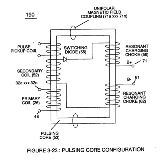](https://stanslegacy.com/uploads/images/gallery/2023-12/kNgKiVhKR3SjdY4I-image-1702696799072-19-56.png)High Voltage Potential of Difference** (Vo - Vn) (SS' - 617 -RR') is accomplished when magnetic flux **lines of force** (71a xx 71n) (Rp) emanating away from closed-loop **magnetic pulsing core** (53) of Figure (190) penetrates Inductance coil-windings (52 - 56 - 62) simultaneously during each and every pulse on-time (T1a xxx T1n) as programmable pulse-train (49a xxx 49n T3 - 49a xxx 49n) is adjusted to "Tune - in" to the dielectric property of **Water** (Re)
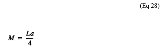
.... causing **mutual inductance** (μ1) (*see equations Eq 28 thru Eq 30*) to transform **Distributed Capacitance** (Cda xxx Cdn) of Figure (7-3) of each **inductance coils** (52 - 56 - 62) into a coherent **Voltage Potential** (Yo •..• Vn) equaling the sum of **Voltage Potential** (Vp) developed across each **Pickup Coils** (VpT + Vp1 + Vp2)
| **Distributed Capacitance** (Cda xxx Cdn) of Figure (7-3)
[](https://stanslegacy.com/uploads/images/gallery/2023-12/LlSOAj47IlZrQIQX-image-1702696921764-21-58.png)[](https://stanslegacy.com/uploads/images/gallery/2023-12/LnZPOrM8WkzklnDw-image-1702523261641.png)
| equations Eq 28 thru Eq 30
Where, (M) is the **mutual inductance** expressed in the same units as (La), (La) is the total inductance of
**Primary coil** (26) and **Secondary coil** (52) with fields aiding.
[](https://stanslegacy.com/uploads/images/gallery/2023-12/orOnPIsU3RdG7LrS-image-1702697017447-23-35.png)
**Coupling Inductance** (Rp) between the **Primary coil** (26) and **Secondary Coil** (52) is further extrapolated in the following equation: Where, (Lt) is the **total inductance**, (L1) and L2) are the **inductance** of each individual **transformer coils** (26)(52), (M) is the **mutual inductance** of each **transformer coil** (26/52) being in parallel relationship with fields aiding.
[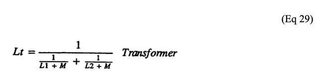](https://stanslegacy.com/uploads/images/gallery/2023-12/T3328JE66oBu2knt-image-1702697029338-23-46.png)
**Coupling Inductance** (Rp1) and (Rp2) in (690) of Figure (7-8) is further expressed in the
following equation: Where, (Lt cc) is the total inductance of **Choke Coils** (FL1 - FL2), (L1) and (L2) are the **inductance** of each individual **choke coil** (56)(62) in series with **Secondary Coil** (52) **Electrical Voltage Potential** (700) of Figure (7-9) and being exposed to the same **Voltage Transformer** (26 - 53 - 52) **magnetic field** (Rp) with aiding fields, (M) is the **mutual inductance** of **choke coils** (L1/L2) since
**Transformer Magnetic Field** (Rp) is the **excitation External Magnetic Field** (Rp1/Rp2) by way of
**Unipolar Pulsing Core** (53).
[](https://stanslegacy.com/uploads/images/gallery/2023-12/eVVovbgNmXNPgC3a-image-1702697038796-23-56.png)
|
... producing **Dynamic Voltage Potential** (600) of Figure (6-3) during repetitive pulsing (49a xxx 49n - T3 - 49a xxx 49n)
... setting up and performing pulsating **Opposite Electrical Attraction Force** (SS' ~ 617 ~ RR' - T3 - SS' ~ 617 - RR') of Figure (7-4) as to **Voltage Dynamics** (220) of Figure (3-29)
| **Opposite Electrical Attraction Force** (SS' ~ 617 ~ RR' - T3 - SS' ~ 617 - RR') of Figure (7-4)
[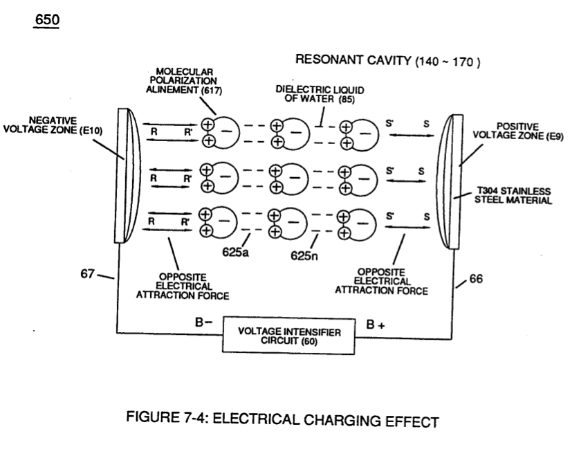](https://stanslegacy.com/uploads/images/gallery/2023-12/30kdftr7xeAN9f0p-image-1702697128032-25-25.png)
| **Voltage Dynamics** (220) of Figure (3-29)
[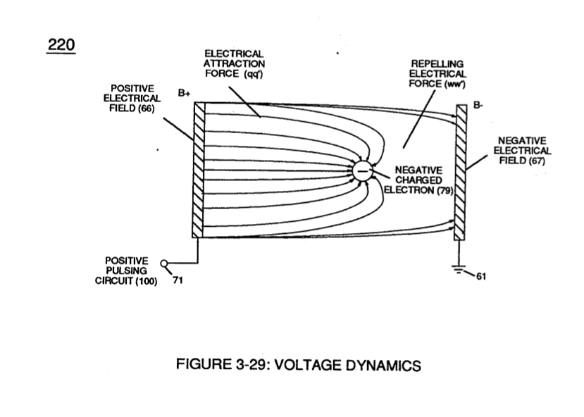](https://stanslegacy.com/uploads/images/gallery/2023-12/61XrnbO4fpkdykfp-image-1702697168227-26-06.png)
|
... triggering **Hydrogen Fracturing Process** (90) of Figure (5-5) as to (100) of Figure (4-8) ... instantly releasing thermal explosive energy (gtnt) (16) from **Water** (85) on demand, as illustrated in **Taper Resonant Cavity** (590) of Figure (6-2) as to (70) of Figure (4-5).
| **Hydrogen Fracturing Process** (90) of Figure (5-5)
[](https://stanslegacy.com/uploads/images/gallery/2023-12/P3Y0jSKB2UWLLZWY-image-1702697249097-27-25.png)
| (100) of Figure (4-8)
[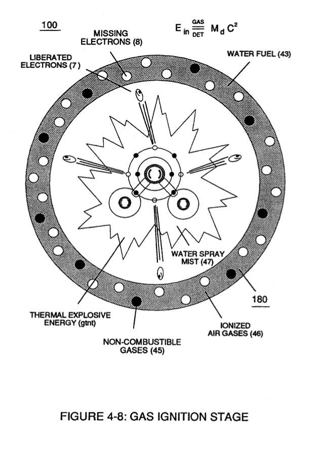](https://stanslegacy.com/uploads/images/gallery/2023-12/0nCgQtWc7OEumvhA-image-1702697290149-28-07.png)
|
| **Taper Resonant Cavity (590) of Figure (6-2)**
[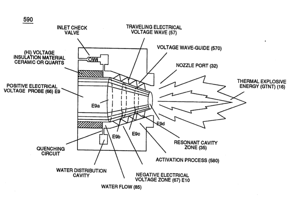](https://stanslegacy.com/uploads/images/gallery/2023-12/iDN6sNT4uVrN1k82-image-1702697335129-28-52.png)
| (70) of Figure (4-5)
[](https://stanslegacy.com/uploads/images/gallery/2023-12/iQtzw2H4BR15Xg4c-image-1702697308683-28-25.png)
|
The resultant **Dynamic Voltage Potential of Difference** (opposite electrical attraction force) (SS' - 617 •... RR') is in balance phase of equal electrical intensity (66 = 67) of opposite polarity (positive electrical voltage potential \_66 equals negative electrical Voltage potential 66 since the **Voltage** **Coefficient of Inductance** (FL1/FL2), **Voltage Coefficient of Capacitance** (Cd1/Cd2), and V**oltage Coefficient of Resistance** (Rs1/Rs2) across choke coils (L1/L2) are the same values
... allowing, **Voltage Bounce Phenomenon** (700) of Figure (7-9) to be preformed.
**Magnetic Field Coupling** (71) of Figure (7-9) entering into and passing through **Secondary Coil**-winding (52) of Figure (7-8) causes and produces copper ions (643a xxx 643n) (Positive Charged atoms 542a xxx 542n having missing electrons) when moving external electromagnetic field strength (71a xxx 71n) is sufficient enough to dislodge electromagnetically charged electrons (641a xxx 641n) from copper atoms making up copper wire material (52).
Collectively, the resultant **positive electrical charged copper ions** (642a xxx 642n) added together produces **Positive Voltage Potential** (629) being electrically applied to **choke-coil** (56);
whereas, the "Liberated" **negative electrical charged electrons** (641a xxx 641n) added together provides **Negative Voltage Potential** (631) to the opposite end of **Secondary Wire** (52) being electrically connected to **choke coil** (62).
Once **Secondary Coil**-winding (52) is de-energized by the removal (collapsing magnetic field during pulse off-time T2 of external **Magnetic Field** (71), the **dislodged electrons** (641a xx 641n) return to **positive charged copper ions** (642a xx 642n)
... terminating and switching off opposite voltage potential (629 - 631) when positive electrical state of the **copper atoms** changes back to net electrical charge of zero.
Sustaining and maintaining the resultant induced **Voltage Potential** (Vo - Vn) without "**Electron Discharged**" (inhibiting electron flow) through **Choke Coil** (62) while, at the same time, inhibiting (preventing) any additional or other electrons from entering into **Secondary copper wire-zone** (52) by way of **Choke Coil** (56) is herein called "**Electron Bounce Phenomenon**" (EbP), as illustrated in (700) of Figure (7-9).
[](https://stanslegacy.com/uploads/images/gallery/2023-12/P3Y0jSKB2UWLLZWY-image-1702697249097-27-25.png)Electrically Interlinked serially together, **Electron Bounce Phenomenon** (EbP), **Voltage Coefficient of Inductance** (F11/F12), **Voltage Coefficient of Capacitance** (Cd1/Cd2), **Voltage Coefficient of Resistance** (Rs1/Rs2), and **Dielectric Coefficient of Water resistance** (Re) allows **Voltage Potential** (Vo - Vn) of opposite electrical polarity to perform work (SS' \_ 617 \_ RR') without amp influxing, thus, not allowing the introduction of electron flow into **Hydrogen Fracturing Process** (90) of Figure (5-5) during **Voltage Stimulation** (SS' - 617 \_ RR')
... causing "**electron clustering**" (641a xxx 641n) to take place within **Copper Wire Zone** (52) during pulse on- time (T1)
... inhibiting "electron flow" to maintain opposite voltage potential (66/E9 \_ 67/E10) across **Resonant Water Gap** (616) during the process of converting water-fuel (85) into instant thermal explosive energy (gtnt)
... therefore, producing a **physical force-yield** (Fy) during gas-ignition (70) of Figure (4-5) which is directly related to the liquid volume of water (85) per injection cycle and applied **Resonant Voltage Intensity** (Yo -Vn), as illustrated in (590) of Figure (6-2) as to (90) of Figure (5-5).
| **physical force-yield** (Fy) during gas-ignition (70) of Figure (4-5)
[](https://stanslegacy.com/uploads/images/gallery/2023-12/iQtzw2H4BR15Xg4c-image-1702697308683-28-25.png)
| (590) of Figure (6-2)
[](https://stanslegacy.com/uploads/images/gallery/2023-12/iDN6sNT4uVrN1k82-image-1702697335129-28-52.png)
|
Of course, in practical terms of component interaction, a minute amount of amp leakage is present and does occur due to **Electronic Component Limitations** but is negligible as to the overall performance of the **Hydrogen Fracturing Process** (590) of Figure (6-2) when being subjected to either one of **Traveling Electrical Voltage Wave**-forms (730 a-b-c) of Figure (7-12), see **Voltage Graph** (750) of Figure (7-14) once again.
| **Traveling Electrical Voltage Wave**-forms (730a - b - c) of Figure (7-12)
[](https://stanslegacy.com/uploads/images/gallery/2023-12/apuQHdvTLUsbYOQ2-image-1702698044180-40-41.png)
| **Voltage Graph** (750) of Figure (7-14)
[](https://stanslegacy.com/uploads/images/gallery/2023-12/1jsle38mbqxsbN9r-image-1702698053508-40-51.png)
|
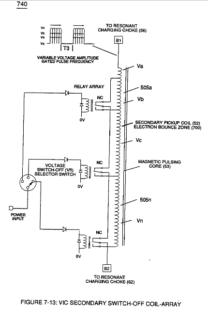
# Voltage Amplitude Switch-Off
**Voltage levels of variance** (Va xxx Vn) is achieved by simply switching-in or switching-out the member of **Secondary Coil**-cavities (505a xx 505n) (see 740 of Figure 7-13) in direct relationship to **Taper Resonant Voltage** **surfaces** (E9/10) of Figure (6-2) which acts and performs as a "**Voltage Amplifier**" when **Compressional Wave-form** (B) of Figure (7-12) is intensified at **Exit Port** (32) of Figure (6-2).
Switching the member of **Secondary Coil-Array** (505a xxx 505n) maximizes electrical power transfer from **Primary Coil** (26) to **Secondary Coil** (52) by keeping **Voltage Amplitude** of **Pulse-train** (49a xx 49n - T3 - 49a xxx 49n) constant.
# Mode of Operability
[](https://stanslegacy.com/uploads/images/gallery/2023-12/sOAwij4rY2PttCc4-image-1702698335874-45-33.png)The established "mode-of-operability" of VIC Coil Assembly (580) of Figure (6-1), now, allows **Voltage Potential** (Vn) of **opposite voltage polarity** (66/SS' - 67/RR') to increase and be attenuated up to and beyond 20 Kilovolts while inhibiting and restricting amp leakage in the milliamperes range
.... establishing operational parameter of utilizing **Opposite Electrical Attraction Force** (SS' - RR') of high voltage intensity (Vn) to instantly release thermal explosive energy (gtnt) from natural water.
**Voltage Compressional Wave-form** (35b) and **Expanding Voltage Waveform** (35c) increases the intensity of applied pulsating opposite electrical attraction force (55'-RR'a xxx SS'-RR'n) even further during each new pulse-cycle (T2 next T2) across water gap (616)
... increasing **Thermal Explosive Energy-yield** (gtnt) to higher energy-levels (gtnta xxx gtntn) beyond applied excitation voltage (Vn) by simply altering **Voltage Surfaces** (35b/35c) as in reference to **Linear Voltage Surfaces** (35a), as illustrated in (730) of Figure (7-12).
**Pulse Off-time** (T2) of Figure (7-8) as to (620) of Figure (7-1) is adjusted to compensate for the rise and fall of magnetic coupling field (71) to produce applied **Unipolar Wave-forms** (64a xxx 64n) entering into **Wave-guides** (35a/35b/35c).
[](https://stanslegacy.com/uploads/images/gallery/2023-12/pmOZtz5IJZzxP9rs-image-1702698415485-46-53.png)
Less water contaminants nets even higher energy-yield (gtnta xxx 85a - 85h xxx gtntn), as illustrated in Water Chart (760) of Figure (7-15).
> In terms of **thermal explosive energy-yield** (gtnt) under dynamic pressure of compression approximately 7.4 (μl) microliter of a liquid-volume of a water droplet per injection cycle is all that is required to run the Dune Buggy 1600cc 50hp VW I.C. engine at 65 m.p.h. on the open road;
>
> whereas, a typical 325 hp diesel I.C. truck-engine would require about 48.1 (μl) microliters of a water droplet per injection cycle to accomplish the same open road performance.
(see WFC Water vs Gasoline Energy Content Equations (memo WFC 429).
[WFC 429 - Optical Thermal Lens](https://stanslegacy.com/books/the-birth-of-new-technology/chapter/wfc-429-optical-thermal-lens)
# WFC 426 - Illustrations
| [](https://stanslegacy.com/uploads/images/gallery/2023-12/N33n4yjmE7kgMcy3-image-1702446340346.png)
| [](https://stanslegacy.com/uploads/images/gallery/2023-12/150OY8ZWHRmLJ4Zc-image-1702446347841.png)
| [](https://stanslegacy.com/uploads/images/gallery/2023-12/hXCKlWYvPKh8fDP4-image-1702446358439.png)
| [](https://stanslegacy.com/uploads/images/gallery/2023-12/qkarW1lNxwhBeV9t-image-1702446367826.png)
|
| [](https://stanslegacy.com/uploads/images/gallery/2023-12/575shrfzd5rBK8Cd-image-1702446379373.png)
| [](https://stanslegacy.com/uploads/images/gallery/2023-12/YkypHSuvzdEmVUF3-image-1702446389842.png)
| [](https://stanslegacy.com/uploads/images/gallery/2023-12/iOu00bYgXilUXFAf-image-1702446398689.png)
| [](https://stanslegacy.com/uploads/images/gallery/2023-12/bAVItVohodNi6mwc-image-1702446407451.png)
|
| [](https://stanslegacy.com/uploads/images/gallery/2023-12/06znou7ARQNGA60Q-image-1702446420154.png)
| [](https://stanslegacy.com/uploads/images/gallery/2023-12/zQ3M8DOyL8aSBVTw-image-1702446431428.png)
| [](https://stanslegacy.com/uploads/images/gallery/2023-12/cMK1JqHzBqOhpF82-image-1702446439945.png)
| [](https://stanslegacy.com/uploads/images/gallery/2023-12/iy2T2mw378gzaURS-image-1702446452554.png)
|
| [](https://stanslegacy.com/uploads/images/gallery/2023-12/GTj6TkpNF3IswUDM-image-1702446469135.png)
| [](https://stanslegacy.com/uploads/images/gallery/2023-12/uVzoZoMe3mI0kWZm-image-1702446478677.png)
| [](https://stanslegacy.com/uploads/images/gallery/2023-12/IF96LOcos6YPtOFi-image-1702446488157.png)
| |