# 8-2 - Traveling Voltage Wave-Guides

![image-1702268827712.png](https://stanslegacy.com/uploads/images/gallery/2023-12/scaled-1680-/Sf3fSg2UAiaH2QZr-image-1702268827712.png)
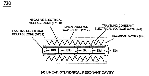
The formation of tubular **Traveling Voltage Wave-guide** (570a) of Figure (7-12) (WFC Memo 426) as to (770) of Figure (8-1) is physically formed when **positive electrical voltage surface** (66/E9) and **negative electrical voltage surface** (67/E10) are placed in <span style="text-decoration: underline;">parallel space relationship</span> to form <span style="text-decoration: underline;">voltage surfaces</span> (E9/E10) <span style="text-decoration: underline;">about an cylindrical axis of rotation having space-gap</span> (35) there between and thus, fanning **Cylindrical Resonant Cavity** (730A) of Figure (7-12) as to (770A) of Figure (8-1) when **space-gap** (616) of Figure (720) exposes **injected water bath** (85) to unipolar pulse-oscillation of high voltage intensity of **opposite polarity** (67/66) as to (780) of Figure (8-2) which, in turn, propagates **opposite electrical attraction force** (RR' \_ 88') of Figure (7-4), as illustrated in (590) of Figure (6-2) as to (585) of Figure (8-1).

<table border="1" id="bkmrk-figure-%287-12%29-%28wfc-m" style="border-collapse: collapse; width: 100%;"><tbody><tr><td style="width: 50.0618%;">(770) of Figure (8-1)![image-1702268946371.png](https://stanslegacy.com/uploads/images/gallery/2023-12/scaled-1680-/Cpp7dgOqjCCin1Ei-image-1702268946371.png)

</td><td class="align-center" style="width: 50.0618%;">(730A) of Figure (7-12)

[![image-1702269030554.png](https://stanslegacy.com/uploads/images/gallery/2023-12/scaled-1680-/UMaHxPz2v93pnLY9-image-1702269030554.png)](https://stanslegacy.com/uploads/images/gallery/2023-12/UMaHxPz2v93pnLY9-image-1702269030554.png)

</td></tr></tbody></table>

<table border="1" id="bkmrk-%28590%29-of-figure-%286-2" style="border-collapse: collapse; width: 100%;"><tbody><tr><td style="width: 49.9383%;">(590) of Figure (6-2)![image-1702269370435.png](https://stanslegacy.com/uploads/images/gallery/2023-12/scaled-1680-/RNfeRJjKbMqMBmxa-image-1702269370435.png)

</td><td style="width: 49.9383%;">(780) of Figure (8-2)

![image-1702269434044.png](https://stanslegacy.com/uploads/images/gallery/2023-12/scaled-1680-/RV66ZRjPslVNpUlL-image-1702269434044.png)

</td></tr></tbody></table>

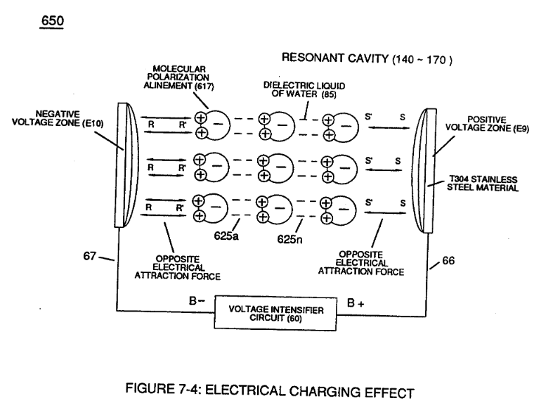
The dielectric property of water (85) (resistance to electron flow) in conjunction with [**VIC Coil Matrix Circuit**](https://stanslegacy.com/books/the-birth-of-new-technology/page/vic-matrix-circuit "VIC Matrix Circuit") (690) of Figure (7-8) (WFC memo 426) as to **VIC Coil Assembly** (580) of Figure (6-1) [(WFC memo 425)](https://stanslegacy.com/books/the-birth-of-new-technology/chapter/wfc-425-taper-resonant-cavity "WFC 425 - Taper Resonant Cavity") ability to inhibit amp "influxing" (**[Electron Bounce Phenomenon](https://stanslegacy.com/books/the-birth-of-new-technology/page/electron-bounce-phenomenon "Electron Bounce Phenomenon") EbP**) during pulsing operations (49a xx 49n) allows voltage amplitude of pulse-frequency potential (T1a xxxT1n) as to (Vo -64a-64b -64c - Vn) of (780A) Figure (8-2) to be applied across cross-sectional circular-ring water bath (85) (donut shape) to cause **Voltage Wave-Form** (57) of Figure (6-2) to <span style="text-decoration: underline;">travel the entire longitudinal length of water-gap</span> (616) since stainless steel material (s/s) (T304) forming Voltage surfaces (E9/E1O) electrically conducts and transfers (**skin effect**) **Voltage Pulse-Freqnency Potential** (583) <span style="text-decoration: underline;">along the inside surface area</span> of the chemically inert and non-oxidizing stainless steel (s/s) tubular material (E9/E1O) <span style="text-decoration: underline;">which physically dictates the shape and configuration of voltage waves</span> (66/67)

... forming tubular voltage wave-guide (s) (570) of Figure (7-12) that, now, becomes the same physical configuration of **Water Gap** (616), as illustrated in (720) of Figure (7-11).

<table border="1" id="bkmrk-%28690%29-of-figure-%287-8" style="border-collapse: collapse; width: 100%; height: 307.033px;"><tbody><tr style="height: 250.233px;"><td style="width: 33.2922%; height: 250.233px;">(690) of Figure (7-8) (WFC memo 426)

[![image-1702269702651.png](https://stanslegacy.com/uploads/images/gallery/2023-12/scaled-1680-/hlsTAFg22rG2oHPG-image-1702269702651.png)](https://stanslegacy.com/uploads/images/gallery/2023-12/hlsTAFg22rG2oHPG-image-1702269702651.png)

</td><td class="align-center" style="width: 33.2922%; height: 250.233px;">(580) of Figure (6-1) (WFC memo 425)

[![image-1702269762692.png](https://stanslegacy.com/uploads/images/gallery/2023-12/scaled-1680-/lpHPcvNC6u1k5L4J-image-1702269762692.png)](https://stanslegacy.com/uploads/images/gallery/2023-12/lpHPcvNC6u1k5L4J-image-1702269762692.png)

</td><td class="align-center" style="width: 33.2922%; height: 250.233px;"> (780A) Figure (8-2)

![image-1702269434044.png](https://stanslegacy.com/uploads/images/gallery/2023-12/scaled-1680-/RV66ZRjPslVNpUlL-image-1702269434044.png)

</td></tr><tr style="height: 56.8px;"><td style="width: 33.2922%; height: 56.8px;">(57) of Figure (6-2)

![image-1702269370435.png](https://stanslegacy.com/uploads/images/gallery/2023-12/scaled-1680-/RNfeRJjKbMqMBmxa-image-1702269370435.png)

</td><td class="align-center" style="width: 33.2922%; height: 56.8px;">(570) of Figure (7-12)

![image-1702268827712.png](https://stanslegacy.com/uploads/images/gallery/2023-12/scaled-1680-/Sf3fSg2UAiaH2QZr-image-1702268827712.png)

</td><td class="align-center" style="width: 33.2922%; height: 56.8px;">(720) of Figure (7-11)

[![image-1702269999016.png](https://stanslegacy.com/uploads/images/gallery/2023-12/scaled-1680-/SSjawAdIQPIrAa1W-image-1702269999016.png)](https://stanslegacy.com/uploads/images/gallery/2023-12/SSjawAdIQPIrAa1W-image-1702269999016.png)

</td></tr></tbody></table>

The <span style="text-decoration: underline;">surface tension of water</span> (584) adjacent to both voltage surfaces (E9 / EI0) <span style="text-decoration: underline;">further aids the transmission of voltage potential</span> (66/67) since **Electrical Charging Effect** (585) of Figure (7-4) <span style="text-decoration: underline;">does not change or alter the dielectric value of water</span> (Re).

[![image-1702270089709.png](https://stanslegacy.com/uploads/images/gallery/2023-12/scaled-1680-/NL2jsNymAkCrRu2O-image-1702270089709.png)](https://stanslegacy.com/uploads/images/gallery/2023-12/NL2jsNymAkCrRu2O-image-1702270089709.png)

<p class="callout info">Together, the **Voltage Coefficient of Water** (e/Eo) of **Equation (Eq 21)** and the **Voltage Coefficient of the stainless steel** (s/s) material fanning voltage surfaces (E9/E10), now, allows the establishment and performance of **Traveling Electrical Voltage Wave-Guide** (583/602) since electrical conductance zone (587) between electrical surface (S) (E9/E10) and the **dielectric surface tension of water** (584) acts and <span style="text-decoration: underline;">performs as a electrical conductor</span> (*Skin Effect*)</p>

[![image-1702270436125.png](https://stanslegacy.com/uploads/images/gallery/2023-12/scaled-1680-/75y1Dd64tmxB7EXs-image-1702270436125.png)](https://stanslegacy.com/uploads/images/gallery/2023-12/75y1Dd64tmxB7EXs-image-1702270436125.png)

... since electrical transmission zone (587) is almost free of electron leakage

...since **Water Bath** (85) is a dielectric-liquid (typically 78.54Q) that <span style="text-decoration: underline;">does not like to transfer nor exchange electrons</span>

<p class="callout success">
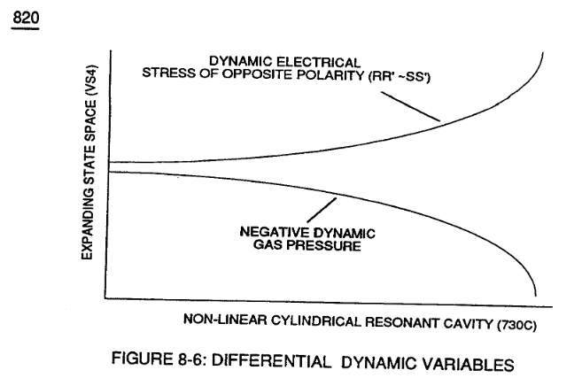
... thereby, maintaining **voltage amplitude potential** (Vo - 64a - 64b - 64c - Vn) of Figure (8-6) without experiencing amp arc-over across **Water-Gap** (616) <span style="text-decoration: underline;">in any appreciable amount</span></p>

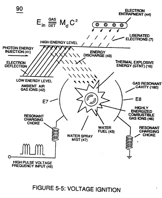
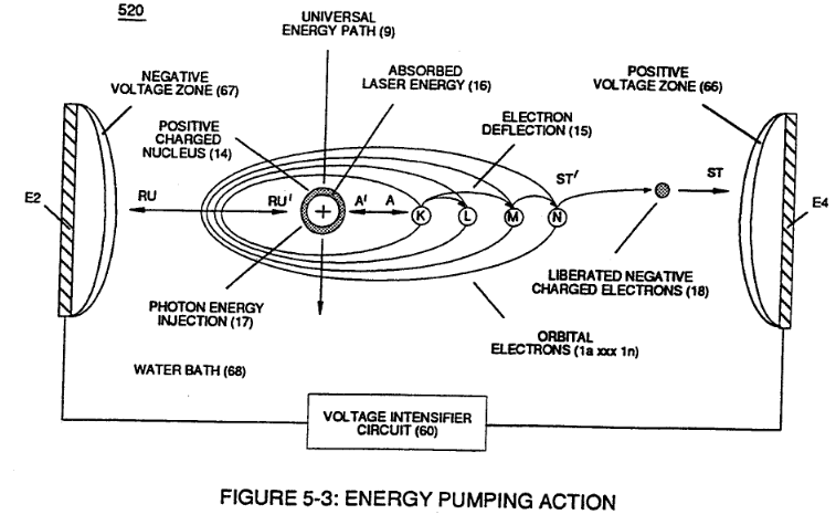
... allowing pulsating opposite electrical attraction forces (RR' / SS') to perform the work of "**Electrically Charging**" water bath (85) to bring-on and trigger **Hydrogen Fracturing Process** (90) of Figure (5-5), as illustrated in **Energy Pumping stage** (520) of Figure (5-3).

<table border="1" id="bkmrk-equation-%28eq-21%29-fig" style="border-collapse: collapse; width: 100%;"><tbody><tr><td class="align-center" style="width: 55.7521%;">Figure (8-6)

[![image-1702270498774.png](https://stanslegacy.com/uploads/images/gallery/2023-12/scaled-1680-/cSWjB8OpUFVJNkvG-image-1702270498774.png)](https://stanslegacy.com/uploads/images/gallery/2023-12/cSWjB8OpUFVJNkvG-image-1702270498774.png)

</td><td style="width: 44.2479%;">(90) of Figure (5-5)

[![image-1702270528283.png](https://stanslegacy.com/uploads/images/gallery/2023-12/scaled-1680-/Ab6wiinjdoj3L05Y-image-1702270528283.png)](https://stanslegacy.com/uploads/images/gallery/2023-12/Ab6wiinjdoj3L05Y-image-1702270528283.png)

</td></tr><tr><td class="align-center" style="width: 55.7521%;">(520) of Figure (5-3)

[![image-1702270566378.png](https://stanslegacy.com/uploads/images/gallery/2023-12/scaled-1680-/xMnZYy37P3CmdRnb-image-1702270566378.png)](https://stanslegacy.com/uploads/images/gallery/2023-12/xMnZYy37P3CmdRnb-image-1702270566378.png)

</td><td style="width: 44.2479%;">  
</td></tr></tbody></table>

**Voltage Intensifier Matrix Circuit** (690) of Figure (7-8) electrically connected with resistive liquid (85/Re) (forming **Resonant Water Gap "**Cp" of Figure 7-8) propagates the transmission of **Traveling Voltage Wave-Form** (57) of Figure (6-2) as to (770) of Figure(8-1) by the functional relationship of **Circuit Resistance Equation** (Eq 9) during programmable **Voltage Pulsing** operations (49a xxx 1'3 xxx 49n) of Figure (8-2).

<table border="1" id="bkmrk-%28690%29-of-figure-%287-8-0" style="border-collapse: collapse; width: 100%; height: 412.533px;"><tbody><tr style="height: 352.933px;"><td class="align-center" style="width: 49.9383%; height: 352.933px;">(690) of Figure (7-8)

[![image-1702269702651.png](https://stanslegacy.com/uploads/images/gallery/2023-12/scaled-1680-/hlsTAFg22rG2oHPG-image-1702269702651.png)](https://stanslegacy.com/uploads/images/gallery/2023-12/hlsTAFg22rG2oHPG-image-1702269702651.png)

</td><td class="align-center" style="width: 49.9383%; height: 352.933px;">Circuit Resistance Equation (Eq 9)

[![image-1702271103815.png](https://stanslegacy.com/uploads/images/gallery/2023-12/scaled-1680-/QFn7lh4KsOWwWemb-image-1702271103815.png)](https://stanslegacy.com/uploads/images/gallery/2023-12/QFn7lh4KsOWwWemb-image-1702271103815.png)

</td></tr><tr style="height: 29.8px;"><td class="align-center" style="width: 49.9383%; height: 29.8px;">(57) of Figure (6-2)

![image-1702269370435.png](https://stanslegacy.com/uploads/images/gallery/2023-12/scaled-1680-/RNfeRJjKbMqMBmxa-image-1702269370435.png)

</td><td class="align-center" style="width: 49.9383%; height: 29.8px;">(770) of Figure(8-1)

![image-1702268946371.png](https://stanslegacy.com/uploads/images/gallery/2023-12/scaled-1680-/Cpp7dgOqjCCin1Ei-image-1702268946371.png)

</td></tr><tr style="height: 29.8px;"><td class="align-center" style="width: 49.9383%; height: 29.8px;">  
</td><td class="align-center" style="width: 49.9383%; height: 29.8px;">Figure (8-2)

[![image-1702271309723.png](https://stanslegacy.com/uploads/images/gallery/2023-12/scaled-1680-/K0frwQoGm9kBtSzp-image-1702271309723.png)](https://stanslegacy.com/uploads/images/gallery/2023-12/K0frwQoGm9kBtSzp-image-1702271309723.png)

</td></tr></tbody></table>