| Figure (7-1) [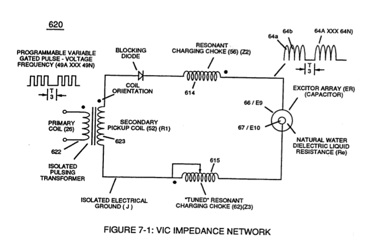](https://stanslegacy.com/uploads/images/gallery/2023-12/sLkFz4mURx82cBMH-image-1702698562791-49-19.png) | Figure (650) of Figure (7-4) [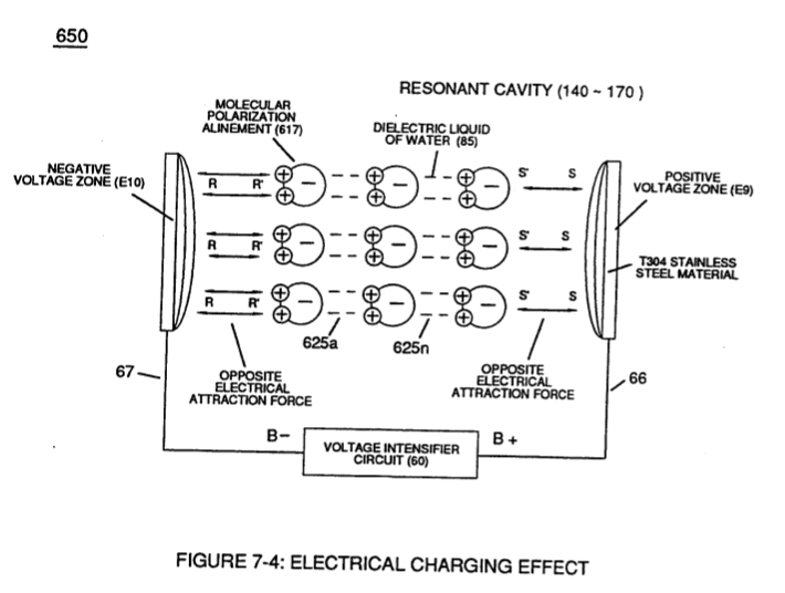](https://stanslegacy.com/uploads/images/gallery/2023-12/b8mwkrkwdlWoaora-image-1702698571159-49-29.png) |
| (720) of Figure (7-11) [](https://stanslegacy.com/uploads/images/gallery/2023-12/8cv37eAtzQtWSpuN-image-1702698583636-49-40.png) | (590) of Figure (6-2) [](https://stanslegacy.com/uploads/images/gallery/2023-12/iDN6sNT4uVrN1k82-image-1702697335129-28-52.png) |
... generally **rain water** (85f) (750) of Figure (7-14) being almost free of contaminates due to **Water Evaporation Process** (532) of Figure (5-6) ... **rain water** (850 being an **liquid-insulator** that restricts the flow of amps
| (750) of Figure (7-14) [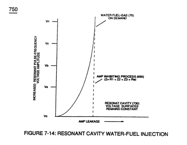](https://stanslegacy.com/uploads/images/gallery/2023-12/rfrUXpva2VKUILHN-image-1702698598868-49-54.png) | (532) of Figure (5-6) [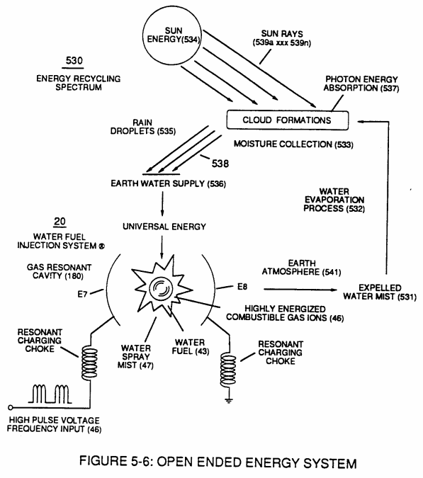](https://stanslegacy.com/uploads/images/gallery/2023-12/79b8QE87ACWFdEZr-image-1702593862699.png) |
| (66/67) of Figure (7-1) [](https://stanslegacy.com/uploads/images/gallery/2023-12/sLkFz4mURx82cBMH-image-1702698562791-49-19.png) | (650) of Figure (7-4) [](https://stanslegacy.com/uploads/images/gallery/2023-12/b8mwkrkwdlWoaora-image-1702698571159-49-29.png) |
In like manner, the stainless steel (s/s) T304 material that forms **Voltage Zones** (E9/EI0) undergo **particle alignment** of its **atomic structure** within the atomic infrastructure of plate-material (E9/E10) when exposed to the same applied electrical voltage fields (66/67) after a pre-set time
... causing **molecular electrical movement** to occur within the surface-material (E9/EI0)
... which, after occurring, the newly formed **molecular electrical orientation** (625a xxx 625n) of Figure (7-4) remains in electrical atomic alignment after pulse off-time (T2) aiding the transference of voltage potential during pulse on-time (T1)
| Figure (7-4) [](https://stanslegacy.com/uploads/images/gallery/2023-12/b8mwkrkwdlWoaora-image-1702698571159-49-29.png) |
| (720) of Figure (7-11) [](https://stanslegacy.com/uploads/images/gallery/2023-12/8cv37eAtzQtWSpuN-image-1702698583636-49-40.png) | (650) of Figure (7-4) [](https://stanslegacy.com/uploads/images/gallery/2023-12/b8mwkrkwdlWoaora-image-1702698571159-49-29.png) |
| Figure (7-1) [](https://stanslegacy.com/uploads/images/gallery/2023-12/sLkFz4mURx82cBMH-image-1702698562791-49-19.png) | (590) of Figure (6-2) [](https://stanslegacy.com/uploads/images/gallery/2023-12/iDN6sNT4uVrN1k82-image-1702697335129-28-52.png) |
| (670) of Figure (7-6) [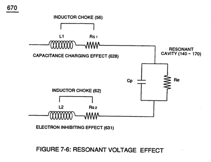](https://stanslegacy.com/uploads/images/gallery/2023-12/HSAV63t6lHwoHa23-image-1702618781512-39-39.png) | (710) of Figure (7-10) [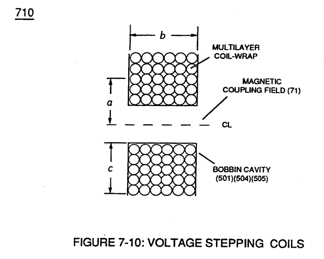](https://stanslegacy.com/uploads/images/gallery/2023-12/ntlSL5wboAbusOLy-image-1702611619154.png) |
| Figure (7-3) as to (580) [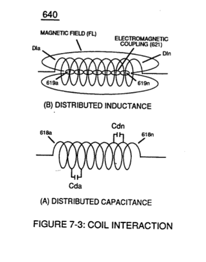](https://stanslegacy.com/uploads/images/gallery/2023-12/LlSOAj47IlZrQIQX-image-1702696921764-21-58.png) | (580) as to Figure (6-1) [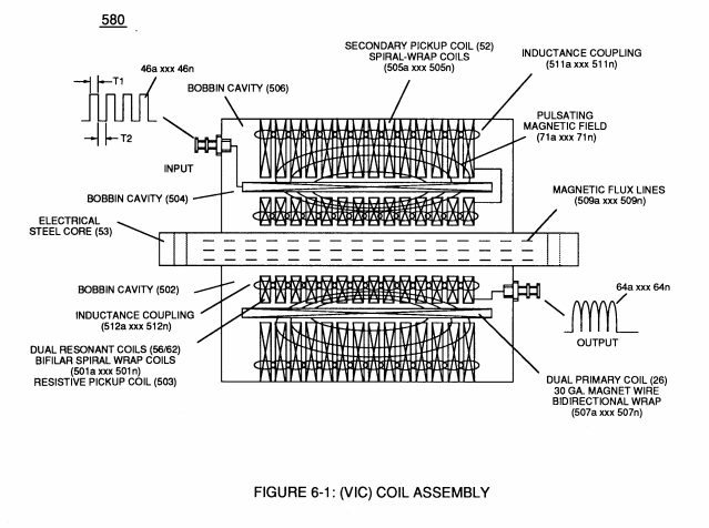](https://stanslegacy.com/uploads/images/gallery/2023-12/nQymCnRuuu9kwxZK-image-1702523026667.png) |
The circular-spiral turns of wire (forming parallel electrical surfaces) is separated by an **Insulated Dielectric Coating Material** which forms a series of capacitors (Cda xxx Cdn) when magnetic flux-lines (619a xxx 619n) produce **Electromagnetic Coupling Field** (621) during pulse on-time (T1), as illustrated in (640) of Figure (7-3) as to (690) of Figure (7-8).
| (640) of Figure (7-3) [](https://stanslegacy.com/uploads/images/gallery/2023-12/LlSOAj47IlZrQIQX-image-1702696921764-21-58.png) | (690) of Figure (7-8) [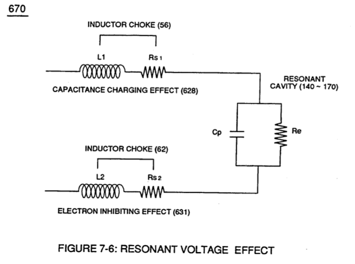](https://stanslegacy.com/uploads/images/gallery/2023-12/rpg6jPD7jlYgCwQs-image-1702618749219-39-07.png) |
| (670) of Figure (7-6) [](https://stanslegacy.com/uploads/images/gallery/2023-12/rpg6jPD7jlYgCwQs-image-1702618749219-39-07.png) | (690) of Figure (7-8) [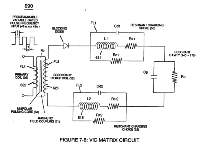](https://stanslegacy.com/uploads/images/gallery/2023-12/pmOZtz5IJZzxP9rs-image-1702698415485-46-53.png) |
**Resonant Charging Chokes** (614/615) 430F/FR 36 AWG (.006) stainless steel (s/s) wire equals **60 micro ohms per centimeter**;
**Primary Coil** (622) 22 AWG (.028) copper wire equals 5.1933 ohms per pound weight;
**Secondary Pickup Coil** (623) 35 AWG (.007) copper wire equals 13K ohms per pound weight.
"**Pyre-ML**" trade name "**Himol**" polymer coating-material is used to impart thermal and mechanical resistance to the stainless steel (s/s) wire (614/615) coating; both magnet wire sizes (622/623) uses solderable **Nysol** (Polyurethane Nylon Jacket) insulation enamel coating as a electrical shield-material
... all dielectric coatings having an effective 3KV per mil dielectric value and formulated specifically to endure automotive temperature range from -40 C to 155 C.