# Capacitance Reactance
**Capacitance Reactance** is determined by the insulation resistance (Rs+Re) and **Inductance** (L1/L2) interacting together during D.C. Pulsing.
Dielectric property of water opposes amp leakage (Re) while another property of water takes-on an "**Electrical Charge**".
Water temperature (Rt) (cool-to-the-touch) keeps (Re) constant since amp flow remains minimal.
**Plate Inductance** (Lc) is **Inductance Reactance** of **Inductor** (L1 ) and **Inductance Reactance** of **Inductor** (L2) in series with **Resonant Capacitor** (140 -170) of Figure (7-6) as to (690) of Figure (7-8).
| **Resonant Capacitor** (140 -170) of Figure (7-6)
[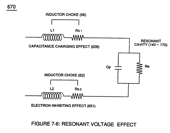](https://stanslegacy.com/uploads/images/gallery/2023-12/9aPfvETrheVTgOak-image-1702613092794.png)
| (690) of Figure (7-8)
[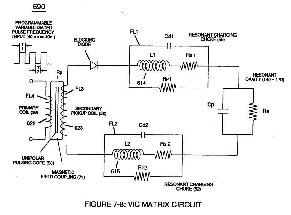](https://stanslegacy.com/uploads/images/gallery/2023-12/gzGVEsezx0gmvk9h-image-1702612335114.png)
|
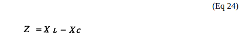
In terms of **Component Reactance**, Inductors (L1/L2) should always be larger than **Capacitor** (ER) of Figure (7-2) in order to maximize amp restriction to enhance "**Voltage Deflection**" (SS' - 617a xxx 617n - RR') of Figure (7-4) and, is expressed by :
| **Capacitor** (ER) of Figure (7-2)
[](https://stanslegacy.com/uploads/images/gallery/2023-12/ld2UDKOKxvKptiGw-image-1702613172661.png)
| "**Voltage Deflection**" of Figure (7-4)
[](https://stanslegacy.com/uploads/images/gallery/2023-12/Dk0i0rZslFjtQ0mh-image-1702613196411.png)
|
[](https://stanslegacy.com/uploads/images/gallery/2023-12/APaEvYdBZl9k2Iyy-image-1702445998069.png)
**Whereas**,
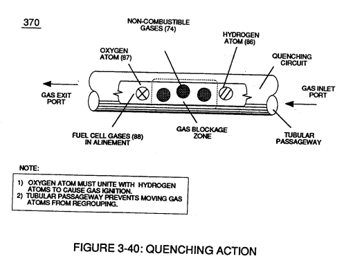
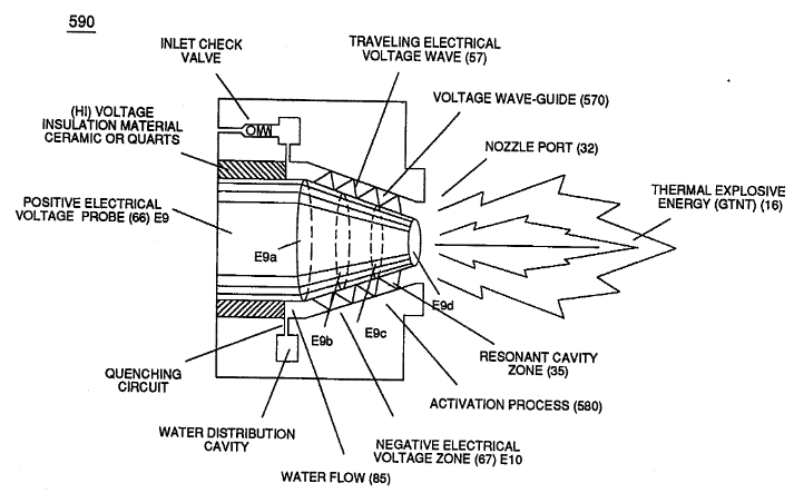
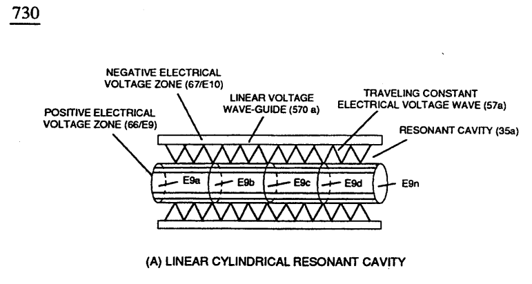
**Capacitor** (ER) should remain relatively small due to the dielectric value of water to obtain maximum **Thermal Explosive Energy-Yield** (16a xxx 16n) of Figure (4-5) and subsequently establishing **Quenching Circuit** (370) of Figure (3-40) to prevent gas ignition inside traveling voltage wave-guide (590) of Figure (6-2) as to (730) of Figure (7-12)
| **Quenching Circuit** (370) of Figure (3-40)
[](https://stanslegacy.com/uploads/images/gallery/2023-12/6YdTq2g8mdXowsG1-image-1702612910404.png)
| (590) of Figure (6-2)
[](https://stanslegacy.com/uploads/images/gallery/2023-12/yfkyykTD8kyZ0ZlP-image-1702321431762.png)
| (730) of Figure (7-12)
[](https://stanslegacy.com/uploads/images/gallery/2023-12/ZPYUzojeavXnoKig-image-1702612413679.png)
|
... to bring-on and trigger Hydrogen Fracturing Process (390) of Figure (3-42) once liberated and expanding water gases (100) of Figure (4-8) passes beyond exit port (E9d)
... activating Voltage Ignition Process (90) of Figure (5-5)
... utilizing **Dynamic Voltage Potential** (600) of Figure (6-3) of opposite electrical stress (SS' - 617 - RR') to cause **thermal atomic agitation** (90) of Figure (4-7) (kinetic heat by atomic motion)
which, when occurring at **gas exit port** (32) of Figure (4-5), spark-ignites expanding water gas-fuel (45/46/47) of Figure (4-5) during water inject cycle (70) of Figure (4-5)
... releasing thermal explosive energy (gtnt) (16) under control state.