| Figure (3-18) [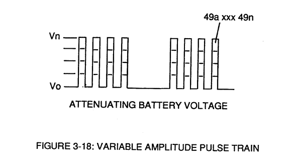](https://stanslegacy.com/uploads/images/gallery/2023-12/perOMBdYqG5zfDB2-image-1703200544967.png) | Figure (3-19) [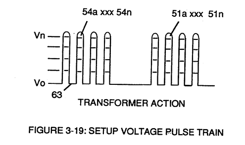](https://stanslegacy.com/uploads/images/gallery/2023-12/UateQAwSqhsH4mKF-image-1703200555466.png) |
However, each **pulse train** (47) (49) are electrically isolated from each other.
Only voltage cross-over from regulated **power supply** (150) of Figure (3-6) to **battery supply** (28) occurs, as illustrated in Figure (3-6).| Figure (3-6)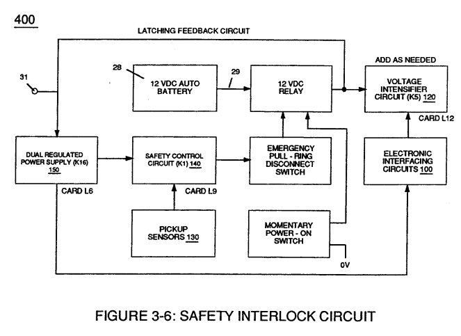 | Figure (3-5)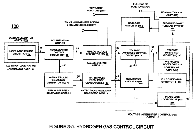 |