# Instant Explosion of Water
The "mode-of-operability" of **VIC Coil Assembly** allows **Voltage Potential** of opposite voltage polarity to increase and be attenuated up to and beyond 20 Kilovolts while inhibiting and restricting amp leakage in the milliamperes range ... establishing operational parameter of utilizing "**Opposite Electrical Attraction Force**" of "high voltage intensity" to "instantly" releases thermal explosive energy (gtnt) from natural water.
The **Voltage Intensifier Circuit** takes advantage of the "**Electron Bounce Phenomenon**" to trigger **Hydrogen Fracturing Process** without amp influxing. **Taper Resonant Cavity** functions as a "**Voltage Amplifier**" when interlinked with **VIC Circuit**.
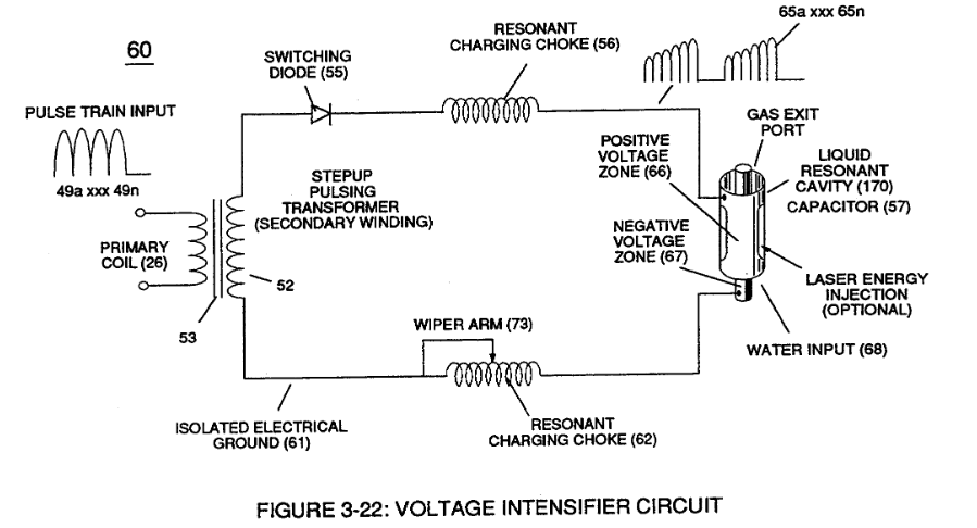
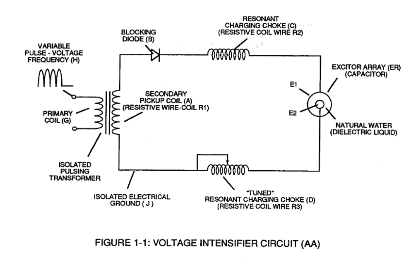
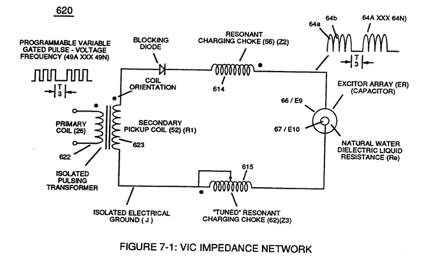
**Voltage Intensifier Circuit** (60) of Figure (3-22) ([Memo WFC 422 DA](https://stanslegacy.com/books/the-birth-of-new-technology/chapter/wfc-422da-wfc-hydrogen-gas-management-system "WFC 422DA - WFC Hydrogen Gas Management System")) as to Figure (1-1) (Memo WFC 420) and **Voltage Intensifier Circuit** (620) of Figure (7-1) are specifically designed to restrict amp flow during **Programmable Pulsing Operations** (49a xxx 49n) but in different operational modes:
| Voltage Intensifier Circuit (60) of Figure (3-22)
[](https://stanslegacy.com/uploads/images/gallery/2023-12/qE3cQ0pxOpRPnR0h-image-1702450549031.png)
| Figure (1-1) (Memo WFC 420)
[](https://stanslegacy.com/uploads/images/gallery/2023-12/nE8xp40ioBIjm8vR-image-1702450578980.png)
| Voltage Intensifier Circuit (620) of Figure (7-1)
[](https://stanslegacy.com/uploads/images/gallery/2023-12/wKUrbHtXacnQw5dk-image-1702450606619.png)
|
VIC voltage circuit (60) utilizes copper wire-wrap to form **Resonant Charging Chokes** (56/62) of Figure (3-22) in conjunction with **Switching Diode** (55) to encourage and make use of "**Electron Bounce**" phenomena (700) of Figure (7-9) to help promote **Step Charging Effect** (628) of Figure (7-7) by preventing electrical discharge of **Resonant Cavity** (140 - 170) since **Blocking Diode** functions as an "**Open**" switch during **Pulse Off-time**;
whereas,
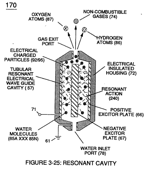
**VIC Voltage Enhancement Circuit** (VIC - VB) (620) of Figure (7-1) incorporates the use of **stainless steel wire-wrap coils** (614/615) to accomplish the formation of unipolar gated pulse-wave (64a xxx T3 xxx 64n) without experiencing "**signal distortion**" or "**signal degradation**" (preventing transformer ringing during signal propagation) as elevated voltage levels ( - xx Vc- xx Vd - xx Vn) while allowing the reduction of **Capacitor-Gap** (Cp) (616) of Figure (7-11) width spacing (57 of Figure 3- 25 ~35 of Figure 6-2) (typically .060 - .010) respectively as illustrated in **Tubular Resonant Cavity** (170) as to **Taper Resonant Cavity (**620) of Figure (7-1).
| (VIC - VB) (620) of Figure (7-1)
[](https://stanslegacy.com/uploads/images/gallery/2023-12/ZEMAYa97rz1qMSUW-image-1702521805142.png)
| (616) of Figure (7-11)
[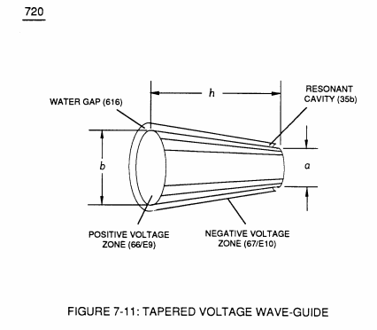](https://stanslegacy.com/uploads/images/gallery/2023-12/XgXLgArcunR7Ioqh-image-1702521824943.png)
|
| (57 of Figure 3- 25 ~35 of Figure 6-2)
[](https://stanslegacy.com/uploads/images/gallery/2023-12/S3eCHXNW0INz4ErI-image-1702447512076.png)
| |
**Switching Diode** (55) of Figure (3-22) prevents Bidirectional electron flow (current flow in one direction only) since **Blocking Diode** (55) only conducts "current flow" in the direction of schematic-arrow while being placed in-line with **VIC Circuit** impedance interaction (R1 + Z2 + Z3 + Re), as mathematically extrapolated in **Circuit Equation** (Eq 9)
... **Diode** (55) being placed between **Secondary Pickup Coil** (52) and **Resonant Charging Choke** (56) to act as an electronic switch in open-position during pulse off-time (**T2**) of Figure (7-8) while preventing electron flow in reverse direction when **Inductor** (L1) **collapsing electromagnetic field** (FL1) produces another **unipolar pulse wave-form** (64a - 64b).
... producing **unipolar voltage wave-form** (64a xxx 64n) during repeated pulse-signal (46a xxx 46n) on-time (T1a xxx T1n)
... allowing the formation of an gated pulse-frequency pulse-train (64a/64b - T3 - 64a/64b) when pulse off-time (T3) is greater than time-period (T2)
... input-signal (49a xxx 49n) being a **Pulse-Train** where (T2) **pulse offtime** (T2) is adjusted to allow **Unipolar Pulse-Train** (64a xxx T3 xxx 64n)
... outputting **Voltage-wave signal** (64a xxx 64n) being a pulse-frequency doubler due to **Inductance Reactance** (FL) of **Inductor Coil** (56) of Figure (3-22) when collapsing magnetic field (FL) of Figure (7-3b) re-cuts **coil-wrap** (Ll) during each pulse off-time (T2)
... producing a second **unipolar voltage wave-form** (64b) during the rise and fall of **magnetic field** (71), as further illustrated in (620) of Figure (7-1)