# Propagating Electrical Stress
As in reference to **WFC Patent Validation Report** dated January 14, 1983 as per **WFC Test-Results** "Mode of Operability" of using "**Voltage Potential**" to "**Dissociates the Water Molecule**" by way of the "**Electrical Polarization Process**" (160) of Figure (3-26) as so specified under U.S. Patent Law (35 USC 101) demonstrate operability, the applied **Pulse-Voltage Frequency** is adjusted to tune-in to the dielectric properties of water by the use of WFC "**Amp Inhibiting Circuit**" (970) of Figure (10-1), as further illustrated in **WFC Tech-Brief** titled "**The Birth of New Technology**"
> ... U.S. Patent Memos 420 - 428, including "Table of Tabulation"
> (Appendix A) as to "Glossary of Application Notes" (Appendix B).
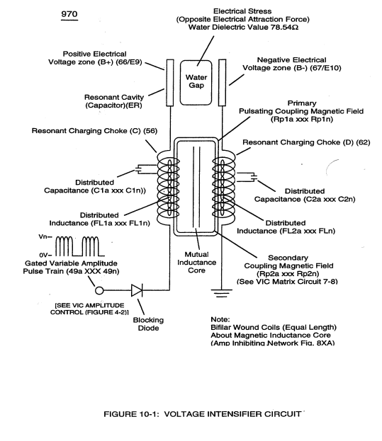
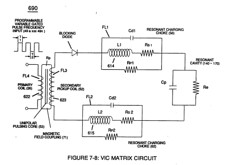
The **Amp Inhibiting Circuit** (970) of Figure (10-1) as to (690) of Figure (7-8) is composed of two copper wires "**Bifilar**" wound (wrapped) about a magnetic induction core to allow amp restriction (minimizing current leakage) while encouraging "**Voltage Potential**"(Va xxx Vn) across the water molecule to perform WFC "**Electrical Polarization Process**", as so illustrated in Figure (7-1) [WFC memo (426)](https://stanslegacy.com/books/the-birth-of-new-technology/chapter/wfc-426-vic-matrix-circuit "WFC 426 - VIC Matrix Circuit") titled **VIC Matrix Circuit**.
| **Amp Inhibiting Circuit** (970) of Figure (10-1)
[](https://stanslegacy.com/uploads/images/gallery/2023-12/0YUyJtuQKZZq8D5H-image-1702939521353.png)
| (690) of Figure (7-8)
[](https://stanslegacy.com/uploads/images/gallery/2023-12/ZT3njPCTon79enNm-image-1702939728729.png)
|
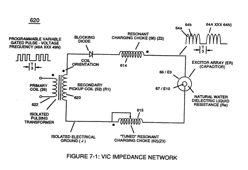
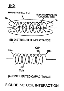
The energized "**Resonant Charging Choke**" (56) of Figure (7-1) as to Figure (10-1) by way of input voltage-pulses (49a xxx 49n) creates an **electromagnetic coupling field** (Rp1) of Figure (7-8) due to its **self-inductance** (640) of Figure 7-3B) crosses over and passes through electrically ground connected **Resonant Charging Choke** (62), as so illustrated in Figure (10-1)
| "**Resonant Charging Choke**" (56) of Figure (7-1)
[](https://stanslegacy.com/uploads/images/gallery/2023-12/Mghp15gu0NRex7m6-image-1702939783175.png)
| **self-inductance** (640) of Figure 7-3B)
[](https://stanslegacy.com/uploads/images/gallery/2023-12/BMbDaBaTU2RN2uZi-image-1702939800001.png)
|
... causing amp flow restriction during each pulsing-cycle since electrons exhibit electromagnetic characteristic
... forming "**Mutual Inductance Fields**" (Rp1/Rp2) once **secondary coil** (62) is electromagnetically energized by **primary coil** (56) and vice versa
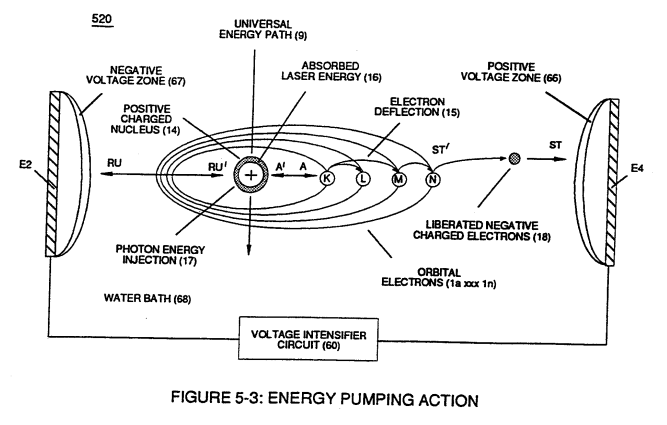
... thereby, preventing amp "in-fluxing" (discouraging electron arc over) across **Dielectric Capacitor Gap** (ER)(66/67) while **Electrical Stress** (ST-ST' - RU-RU') of **Opposite Voltage Polarity** (B+/B-) brings on **Energy Priming Stage** (520) of Figure (5-3) which is refer to, herein, as "**Voltage Tickling of State Space**."
| **Energy Priming Stage** (520) of Figure (5-3)
[](https://stanslegacy.com/uploads/images/gallery/2023-12/60fKlYumsAqhz4DV-image-1702942966128.png)
|
The resultant **Amp Inhibiting Circuit** Figure (10-1) as to Figure (10-3 A/B) further allows amp restriction (minimizing current leakage) to be continued even if applied "**Voltage Amplitude**" is increased. The length and diameter size of the copper-wire spiral wrapped coil (56/62) of Figure (10-1) being paired together and electrically energized in conjunction with applied **Voltage Pulse-Frequency** determines how much "**Amp Leakage**" will occur across capacitor **Gap** (Cp) while "**Voltage Pulse-Potential**" (Va xxx Vn/49a xxx 49n) of "**Opposite polarity**" (B+/B-) is/are allowed to be applied across "**Electrical Voltage Plates**" (Voltage-Zones) (66/67).
| **Amp Inhibiting Circuit** Figure (10-1)
[](https://stanslegacy.com/uploads/images/gallery/2023-12/0YUyJtuQKZZq8D5H-image-1702939521353.png)
| Figure (10-3 A/B)
[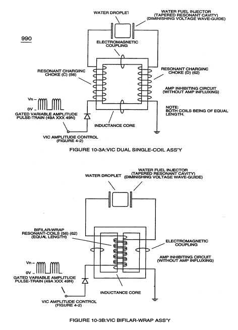](https://stanslegacy.com/uploads/images/gallery/2023-12/KXhbKB5X4AfEU0Lz-image-1702942909160.png)
|
To reduce amp leakage still further, the copper wire of both **Resonant Charging Chokes** (56/62) can be replaced with a magnetically inductive stainless steel wire (430F/FR) having a resistive value (Ohms) to the flow of electrons while taking on the capacitance and inductance characteristic of a coil wire.
VIC **Bifilar Wrap Coil-Assembly** (10-3B) and VIC **Dual Coil Wrap-Assembly** (10-3A) both utilize either "E" & “I” and "U" Inductance Core configurations to concentrate Mutual Inductance Fields (Rpl/Rp2) in order to optimize **Amp Inhibiting Process** (750) of Figure (7-14).
[](https://stanslegacy.com/uploads/images/gallery/2023-12/GohHkqjrGXbkNPrN-image-1702939496250.png)"E" “I” core shape (10-3B) is **most preferable** since amp spike surge is minimize during repetitive pulsing operations.
[](https://stanslegacy.com/uploads/images/gallery/2023-12/0YUyJtuQKZZq8D5H-image-1702939521353.png)Beyond amp restricting characteristic of said **Amp Inhibiting Circuit** (970) of Figure (10-1) as to **Voltage Intensifier Circuit** (60) of Figure (3-22), the spiral-wrapped coils (**Resonant Charging Chokes** 56/62) being paired together, also, causes voltage level enhancement beyond applied voltage input since the "**Distributed Capacitance**" (C1a xxx C1n - C2a xxx C2n) / "**Distributed Inductance**" (FL1a xxx FL1n - FL2a xxx FL2n) of said "bifilar" wrapped coils (Figure 7-3) as to (990) of Figure (10-3) encourages the compounding effect (increasing magnetic field-strength during each pulsing cycle) of electromagnetic field-strength (Rp1a xxx Rp1n - Rp2a xxx Rp2n) (mutual induction) when applied **Pulse-Voltage** frequency (49a xxx 49n) of Figure (3-34) passes through the positive energized **Resonant Charging Choke** (56).
Furthermore, the paired coil-wires opposite voltage potential \[**positive electrical attraction force** (B+) - **negative electrical attraction force** (B-)\] \[hereinafter called **Electrical Stress** (SS' - RR') as to (160) of Figure (3-26)\] are always **equal** in electrical magnitude/intensity **since the wire-lengths of each coil** **are the same**.
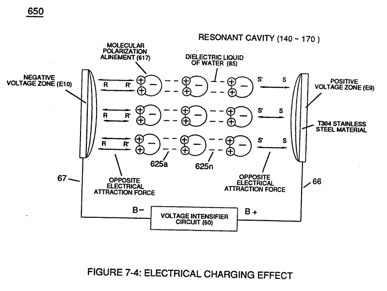
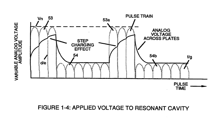
**Pulse-Voltage** repetition rate sets up the step-up charging effect Figure (1-3) since the "**Resonant Cavity**" (Cp) functions as a "**Capacitor**" (ER) due to the dielectric value of the liquid (or gases) which becomes an integral part of the **VIC Circuit**, as so illustrated in (650) of Figure (7-4).
[](https://stanslegacy.com/uploads/images/gallery/2023-12/gvwO7lLymg5QDCCF-image-1702942582537.png)
The resultant voltage enhancement (**Voltage Amplitude**) can *exceed 40 kilovolts* to instantly convert water (droplets) into thermal explosive energy (gtnt) on demand, as so illustrated in **Voltage Intensifier Circuit Diagram** (970) of Figure (10-1).
**[](https://stanslegacy.com/uploads/images/gallery/2023-12/0YUyJtuQKZZq8D5H-image-1702939521353.png)**
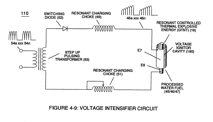
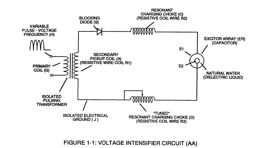
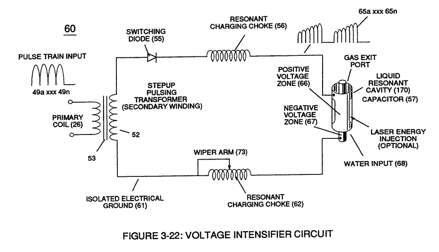
**Blocking Diode** (52) of Figure (4-9) as to Figure (1-1) allows **unipolar pulse-wave** to go more positive on each pulse-cycle since the **Blocking Diode** (52) prevents the **Resonant Cavity** (Cp) from discharging during pulse off-time, as so illustrated in Figure (1-4) as to (60) of Figure (3-22)
| **Blocking Diode** (52) of Figure (4-9)
[](https://stanslegacy.com/uploads/images/gallery/2023-12/UUWbK3PTfcFQX1x5-image-1702942719974.png)
| Figure (1-1)
[](https://stanslegacy.com/uploads/images/gallery/2023-12/SKQ3lhwFMYNvXMGW-image-1702942745761.png)
|
| **Figure (1-4)**
[](https://stanslegacy.com/uploads/images/gallery/2023-12/SgHtDkV4j5pRs7ws-image-1702942767454.png)
| (60) of Figure (3-22)
[](https://stanslegacy.com/uploads/images/gallery/2023-12/Pn4vejGyLzXDQAka-image-1702942693073.png)
|
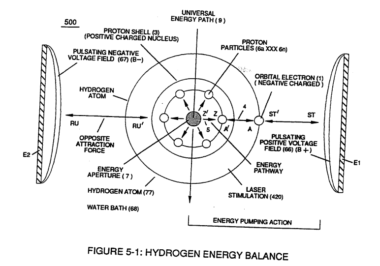
... allowing the developed "**Electrical Stress**" (RU/RU' - ST/ST') of Figure (5-1/5-2) across **Capacitor Gap** (Cp) to go to the farthest point beyond the "**State of Equilibrium**"
> ... see [Atomic Energy Balance of Water (WFC memo 424)](https://stanslegacy.com/books/the-birth-of-new-technology/chapter/wfc-424-atomic-energy-balance-of-water "WFC 424 - Atomic Energy Balance of Water"), once again.
[](https://stanslegacy.com/uploads/images/gallery/2023-12/0YUyJtuQKZZq8D5H-image-1702939521353.png)
The programmable pulse-frequency (49a xxx 49n) of Figure (10-1) input is simply adjusted to tune-in to the dielectric property of the **Water Molecule**.
The resultant **Dynamic Electrical Charging Effect** (612) of Figure (8-1) acts as a progressive energy enhancer (**Energy Priming Stage**) (500) of Figure (5-1)
| **Dynamic Electrical Charging Effect** (612) of Figure (8-1)
[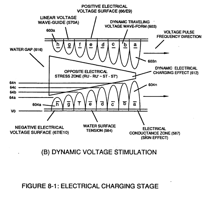](https://stanslegacy.com/uploads/images/gallery/2023-12/jbE7xDLZED0syEvn-image-1702942166357.png)
| **Energy Priming Stage** (500) of Figure (5-1)
[](https://stanslegacy.com/uploads/images/gallery/2023-12/xaTVEqFGT7fB4FVF-image-1702942202139.png)
|
when **Static State Space** (790) of (8-3) is configured to **Dynamic State Space** (800) of Figure (8-4), as so illustrated in [WFC memo (427)](https://stanslegacy.com/books/the-birth-of-new-technology/chapter/wfc-427-voltage-wave-guides "WFC 427 - Voltage Wave Guides") titled "**Voltage Wave-Guide**"
| **Static State Space** (790) of (8-3)
[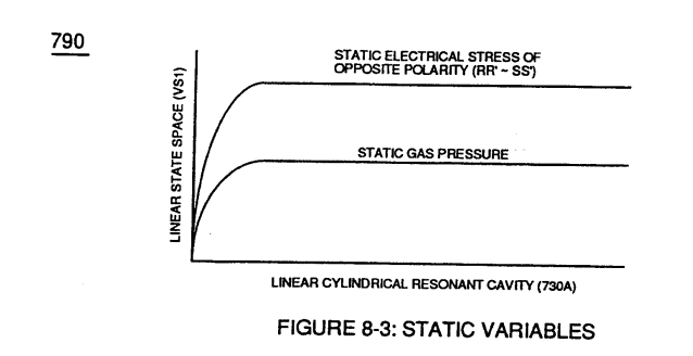](https://stanslegacy.com/uploads/images/gallery/2023-12/79jfPp35lIj536Tg-image-1702942388172.png)
| **Dynamic State Space** (800) of Figure (8-4)
[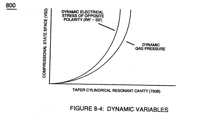](https://stanslegacy.com/uploads/images/gallery/2023-12/LJTBdQOkTdGKfIIe-image-1702942399614.png)
|
... whereby, the **Voltage Wave-Guides** forms **Water Gap** (Cp).