# Taper Resonant Capacitor (ERt)
**Capacitor** (ER) is automatically formed when dielectric liquid of water (Re) is placed between **Electrical Conducting Plates** (E1/E2) of Figure (1-1) page (1-13) ([Memo WFC 420](https://stanslegacy.com/books/the-birth-of-new-technology/chapter/wfc-420-hydrogen-fracturing-process "WFC 420 - Hydrogen Fracturing Process")).
Stainless steel T304 material is used to form **Electrical Voltage-Plates** (EIIE2) which do "not" chemically interact (chemically inert) (Lab tested less than .0001/year decomposition rate) with liberated water gases (hydrogen \_86, oxygen \_87, and non-combustible gases W being exposed to an high intensity voltage pulse-field (64a xxx 64n) with negligible amp flow.
**Electrical Plates** herein called "**Excitor**" Plates or **Voltage Zones** (E1/E2) can take-on different configuration of shapes to maximize **Dynamic Voltage Potential** (600) of Figure (6-3) for different application of usage:
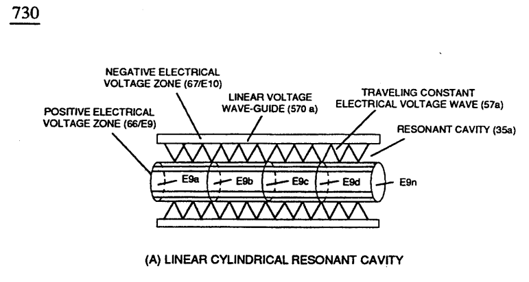
(35a) **Traveling Constant Electrical Voltage Wave** by way of linear cylindrical resonant cavity (Tubular Cavity 730A),
(35b) **Traveling Compressional** (concentrating electrical intensity) **Electrical Voltage Wave** by way of taper cylindrical resonant cavity (730B),
(35c) **Traveling Expanding Electrical Voltage** wave by way of non-linear cylindrical resonant cavity (730C)
... or any voltage surface combination thereof
... each resonant cavity design acting and functioning as a **Voltage Wave-guide** (570) and gap-size (35) sufficient enough to allow the "**Quenching Effect**" to take place, as illustrated in (730) of Figure (7-12) as to (370) of Figure (3-40).
| (730) of Figure (7-12)
[](https://stanslegacy.com/uploads/images/gallery/2023-12/ZPYUzojeavXnoKig-image-1702612413679.png)
| (370) of Figure (3-40)
[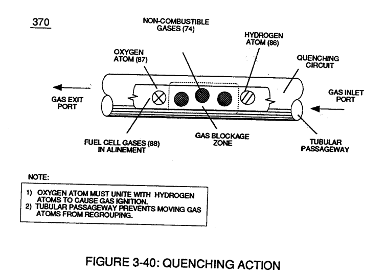](https://stanslegacy.com/uploads/images/gallery/2023-12/8G6ENOaauv9BUBR9-image-1702612439452.png)
|
The dielectric property of water (being 78.54 ohms @ 25° C) permits the storage of '"**Electrical Charge**" when a potential voltage difference exists between **Electrical Voltage-Plates** (E1/E2) as to (E9/E10).
**[](https://stanslegacy.com/uploads/images/gallery/2023-12/FWz40QLyPOJwJefG-image-1702595701485.png)**
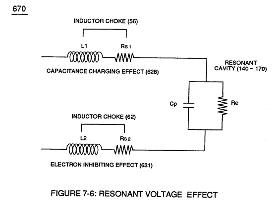
**Capacitance** (Cp) of Figure (7-6) as to (690) of Figure (7-8) is determined by the surface area (A) of **Electrical Voltage-Plates** (E1/E2 - E9/E10), the distance (d) between the **Electrical Plates** (in inches), and the **permittivity** (Eo) of the dielectric property of water (85) and, is expressed in the following equation:
**Where**,
(Eo) is **Free-Space Permittivity of Water** established by **VIC Circuit** (690) of Figure (7-8) ability to restrict amp flow,
(e/Eo) Ratio is the **Dielectric Constant of Water**,
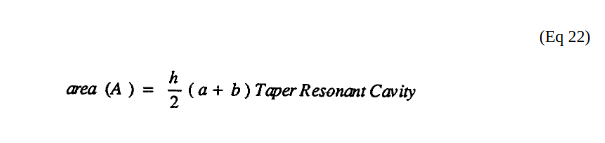
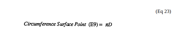
(A) is the surface Area of **Resonant Cavity** and, is expressed in the below equation:
[](https://stanslegacy.com/uploads/images/gallery/2023-12/7DDADpHgskHekyV1-image-1702445610200.png)
**Where**,
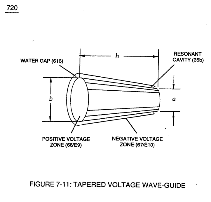
(h) is longitudinal length of tapered resonant cavity,
(a) being exit pan circumference surface point (E9d) of Figure (6-2),
(b) being cylindrical circumference surface point (E9a) of Figure (6-2) where tapered surface starts,
(a) (b) circumference surface points (E9a)(E9d) respectively determined by below expressed equation:
(see diagram 720 of Figure 7-11)
[](https://stanslegacy.com/uploads/images/gallery/2023-12/nGqEpPvBXerFXvQV-image-1702445834337.png)
**Where,**
(D) is diameter cross section of cylindrical surface at designated point (E9a - E9n),
(x) being mathematical constant 3.1416.
| diagram 720 of Figure 7-11
[](https://stanslegacy.com/uploads/images/gallery/2023-12/nZspZRIZeJzET3th-image-1702612195058.png)
|