
Step Charge as a function of Pulse Period
Here we can see the Cell Driver Circuit pulsing a double cell in parallel. The arrangement is powered by a 12V ATX supply. The Cell Driver's inputs: Vcc and Vee are both B+ 12VDC REG. The primary coil is replaced with the LC load of the cell & a 39mH iron core inductor, either using the centertap or the full coil. (12-0-12 side of a 6:1 stepdown. 120V side at 612mH). The water in the cell was old well water. (new tests are needed with fresh and/or distilled water)
Parameters of Test:
Width: 1388 uS
Space: 760 uSF = 1/S
F = 1 / (0.001388 + 0.000760) = 1 / 0.002148 uS
F = ~465 Hz ?Gate Spacing (2466 uS or 2.466mS)
Inductor: 17.5mH (half of a 12-0-12 stepdown at 39mH total)
DMM Measured Resistance 12-0-12: 0.6R each half, and 1.3R full coil
B+ Voltage applied to cell: 12V REG (from ATX supply)
Transformer used as inductor: Jameco Valuepro 67-1242 Center-Tapped Power Transformer, 24 VAC, 48 Watt, 2 Amps, 2.60" H x 4.10" W x 2.50" L
This inductor appears to be playing the role of Vc2. When I introduce a mutually coupled Vc1 (the other side of the core at 612mH), regardless of phase, all modulation and/or rise is completely dampened.
Too large of an inductance at the Vc2 position (in this specific arrangement), dampens out all modulation.
Too small of an inductance at the Vc2 position (etc), allows much more of the pulse to be reproduced at the load Vout, and "Cell Saturation" is perhaps reached too soon.
Too large of an inductance in a Vc1 position also significantly inhibits modulation, unless sufficient offsetting capacitance is added in the form of parasitics, distributed coupling or external parallel capacitance.
Perhaps this is the reason for the inverted pulse trains feeding the Cell Driver input. If a constant DC bias during "offtime" is applied, then during the pulse pull down, inductive reversal directed by the diode, is responsible for the higher voltage spikes.
This process cumulatively increases the bias of the cell cathode with each successive pulse by allowing the energy to store in the negative (side) inductance. The voltage will rise (return) up to at least the available source voltage, or higher with the spikes. Given a higher voltage input, it seems quite possible that the 8XA style variac power supply, with added filtering, could supply the load directly (replacing the 12V REG here), up to 60VDC at least regarding the TIP120 thresholds (100V TIP122). Utilizing a higher voltage input would presumably result in much higher amplitude spikes, with the same 2.5V threshold, which appears to be the forward voltage drop across the TIP Collector/Emitter junction.
(Edit: Don't use a variac. It will blow something up. Instead, we should look at using a 0-60VDC supply, with an addition 7812 12V Regulator to supply the Vcc/Vee to the Cell Driver. This will keep everything on the same bonded ground, and safe for operation)
With this operation in mind, and in this configuration, I can now appreciate the design of Max Miller's digitally controlled power supply board, and its inverted output pulsing. The cell driver TIP120, in this case, acts as a low side switch on the cell, and is rendered safer to operate, by existing electrically further away from the B+ voltage source. The NPN junction is not subject to a large voltage differential during switching. The voltage dropped across the inline cell and inductor significantly reduces the remaining voltage to be dropped across the junction.
What we see here:
|
What we don't see here:
|
Schematic for arrangement
Edit: Inductor is 39mH and circuit operation used the center-tap for an equivalent inductance of 19.5mH
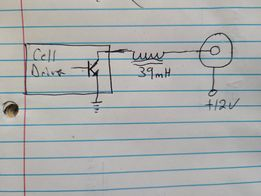
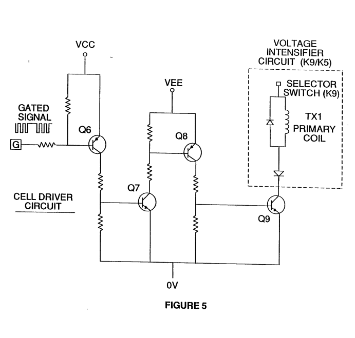
Cell Driver Circuit
UPDATE: 7/4/22
Swapping out the freshly conditioned new cell, for the old double barrel, and using the same inductance, caused a shift in the saturation limit of the step-charge. The old cell exhibited almost too much dampening, and significantly less bubbles were the result. Pulse width had to be reduced to levels under 500uS in order to regain the stepcharge. At which point, the amplitude also suffered, suggesting an adjustment to inductance is required.
More tests are needed with other cells and inductances to determine where the largest headroom (width vs. count) exists, allowing the highest source amplitude possible, to be reached.