

article
The Electrical Measurement of Molecular Junctions (Reed, Zhou, Tour et al., 1998)
23 September 2026
The Electrical Measurement of Molecular Junctions
M. A. Reed, C. Zhou, M. R. Deshpande and C. J. Muller, Center for Microelectronic Materials and Structures, Yale University; T. P. Burgin, L. Jones II and J. M. Tour, Department of Chemistry and Biochemistry, University of South Carolina. Annals of the New York Academy of Sciences, volume 852 (Molecular Electronics: Science and Technology), June 1998, pages 133–144. doi:10.1111/j.1749-6632.1998.tb09868.x.
Why the archive holds it
Meyer explains his cell one molecule at a time: voltage pulls on the water molecule's electrons and the molecule comes apart. This paper shows what it takes to put electricity through one molecule and measure it. It was written in the same years as his last papers, by the Yale group that first did it, with James Tour, who made the molecules. The same measurement was published in Science in October 1997. This version gives more of the method and adds a second device.
The paper is not about water, and it does not test anything Meyer claimed. The molecules are benzene-1,4-dithiol and a biphenyl thiol, dried in argon, between gold contacts. Nothing is split and no gas is made. What it gives a reader of Meyer is measured scale: what "a molecule between two electrodes" looks like electrically when someone actually builds one.
What to take from it
- A single molecule is a very small capacitor with a threshold. The current does not flow until about 0.7 V is across the junction (Figure 4). Read as a charging gap, that implies a capacitance of 1.1 × 10⁻¹⁹ F. Their crude model of a small metal sphere between two plates gives 0.4 × 10⁻¹⁹ F. The threshold is roughly the voltage needed to put one extra electron onto that capacitance (e/2C ≈ 0.73 V). The authors also give a second explanation: the gold's Fermi level does not line up with the molecule's lowest empty orbital. They do not decide between the two.
- One molecule measured about 22 megohms. The highest resistance they ever saw was about 22 MΩ. Once they saw about half that, which they read as two molecules side by side. The 22 MΩ figure is the reason they believe a single molecule was in the gap.
- The contacts decide the direction. Their second device puts a monolayer of molecules between a gold electrode and a titanium one. It passes current about 500 times more easily one way than the other (Figure 6). One way, electrons are thermally emitted over a 0.26 eV barrier at the titanium side. The other way, they hop from site to site with a 0.19 eV activation energy. Both molecules and metals were chosen on purpose, and the result depends on the metal on each side of the molecules.
- It needed extreme care to see anything. The gap had to be held steady to picometres, which is why they used a break junction. The monolayer took three days to form, the metal went on at 0.3 Å a second, and the samples warmed up over a day. Without the molecules, dry vacuum tunnelling showed "a much higher resistance". Wet solvent alone conducted ionically at 1–2 GΩ.
The transcription below keeps the printed text, including its slips: "the current at −1 V bias is about 500 times higher than the current at −1 V bias" (one of the two should be +1 V), "as shown in FIGURE 3(b)" for Figure 7(b), "reprodicibility", "300 A" for 300 Å, "l/T" for 1/T, and reference 6 given as Phys. Rev. Lett. with a Phys. Rev. B page number. The eight figures are cropped from the printed pages.
Abstract: We present the investigation of the electrical transport of metal/(organic molecule or monolayer)/metal junctions. Utilizing a novel mechanically controllable break junction to form a statically stable system, we have self-assembled molecules of benzene-1,4-dithiol onto two facing gold electrodes allowing for direct observation of charge transport through the molecules. Current-voltage I(V) measurements provides a quantitative measure of the conductance of a junction containing a single molecule. We have also created a technique to form well-defined, stable, and reproducible metallic contacts to a self-assembled monolayer of 4-thioacetylbiphenyl with nanoscale area. Electronic transport measurements show a prominent rectifying behavior arising from the asymmetry of the molecular heterostructure. Variable-temperature measurements reveal the dominant transport mechanisms, such as thermionic emission for the Ti-organic system. These techniques demonstrate the capability of electrically characterizing and engineering conductive molecular systems for future potential device applications.
The measurement of charge transport in single organic molecules, and the determination of their conductance, is a long-sought goal. Such measurements are experimentally challenging and intriguing since one can test the validity of transport approximations at the molecular level. A conceptually simple configuration would be to connect a single molecule between metallic contacts. Such a metal-molecule-metal configuration would present the molecular embodiment of a system analogous to a quantum dot,1–9 with the potential barriers of the semiconductor system replaced by any existing contact barrier of the molecule/metal interface. Previous measurements on atomic and molecular systems have been done by scanning tunneling microscopes (STM),10–12 and can yield conductivity information.13–15 Experiments with an evaporated-metal-top contact/molecules/metallic-bottom-contact configuration, which has ten of thousands of parallel active molecules, have also been demonstrated.16,17 One experiment on an organic system18 reported evidence for Coulomb charging. We have performed measurements in the configuration of a single molecule between metallic contacts; specifically on benzene-1,4-dithiolate connected between stable proximal metallic gold contacts, at room temperature. This approach complements previous approaches by presenting statically stable contacts, and concurrently restricts the number of active molecule(s) to as few as one.
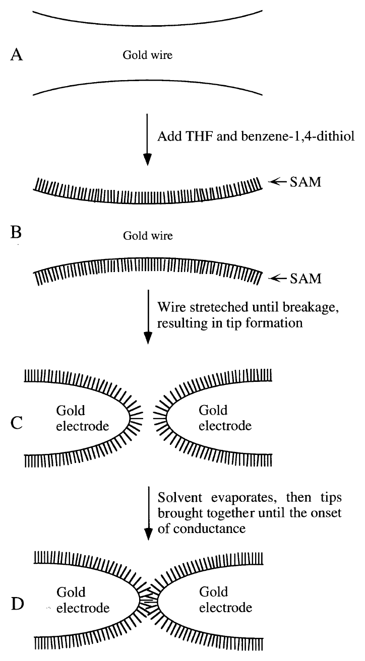
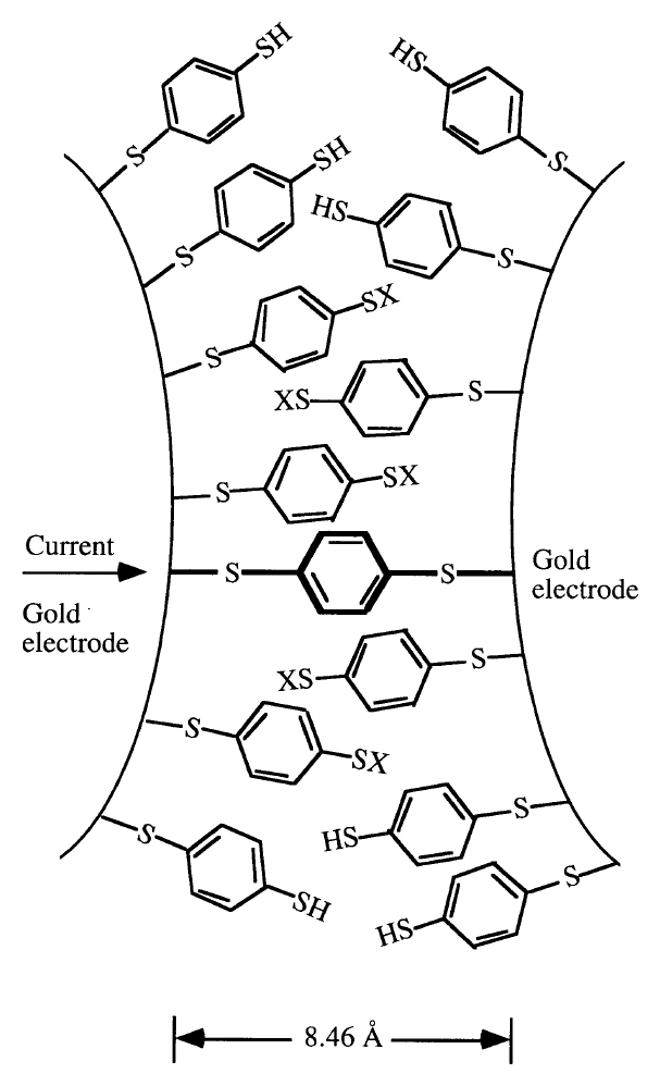
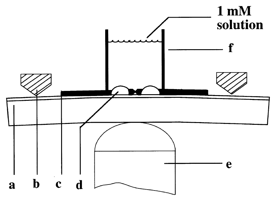Experiments were conducted at room temperature using a mechanically controllable break junction (MCB)19 (Fig. 1). In this approach, a notched metal wire is glued onto a flexible substrate and is fractured by bending the substrate, after which an adjustable tunneling gap can be established. A large reduction factor between the piezo elongation and the electrode separation ensures an inherently stable contact or tunnel junction. The wire contacts are atomically sharp when broken, demonstrated in the conductance quantization as previously reported.20 In the experiments reported here, benzene-1,4-dithiol was adsorbed from a 1-millimolar (mM) solution in tetrahydrofuran (THF) onto the two facing gold electrodes of the break junction broken in solution under an Ar atmosphere,21 resulting in formation of a self-assembled monolayer (SAM) on the gold electrodes nearly perpendicular to the surface.21 The THF solvent was allowed to evaporate in the ambient Ar atmosphere prior to the conductance measurements, and there was no further surface preparation or cleaning. The removal of the THF led to thermal gradients, which disturbed the picometer static dimensional stability of the MCB, requiring the tips to be withdrawn and then returned to measure the electrical properties of the molecule(s) adsorbed on the surfaces (Fig. 2). The configuration of Figure 3 is probable, since the displacement of thiols has been shown,10 and the formation of a disulfide bridge would require oxygen.21
As the tips were brought together, current-voltage I(V) and conductance G(V) (= dI/dV) measurements showed characteristic features (Fig. 4A) which proved to be highly reproducible (Fig. 4B). The spacing between the electrodes is ∼8 Å, set by the piezo voltage as determined by previous calibration of the spacing-to-piezo voltage conversion factor established by the exponential dependence of the current with distance in the tunneling regime.22 However, calibration shift due to the solvent evaporation cannot be eliminated. By comparison, an approximate molecule length of 8.46 Å was calculated using an MM2 force field and measuring to the center of the two gold radii minus the covalent radii of both gold atoms. An apparent gap of ∼0.7 V was observed in all cases. The first derivative of I(V) shows two steps in both bias directions with the lower step ∼22.2 Mohm (0.045 µS) and the higher step ∼13.3 Mohm (0.075 µS), possibly indicative of a Coulomb staircase. It is noted that the high Fermi energy of the gold contacts (∼2 eV) as compared to the low energies of semiconductor quantum dot systems (<100 meV) precludes the observation of negative differential resistance in the present system,23 which is often seen in semiconductor systems.1–7 A control experiment with unevaporated THF solvent alone (that is, without the benzene-1,4-dithiolate) exhibited a resistance of 1-2 Gohm (linear up to 10V independent of electrode spacing, implying ionic conduction through the solvent. When the solvent was evaporated, regular vacuum tunneling with a much higher resistance was observed,19 with exponential dependence of the current with applied voltage implying the absence of deleterious effects on the MCB due to the solvent. The first step for these three measurements gives resistance values of 22.2, 22.2, and 22.7 Mohm (top to bottom); the next step gives resistance values of 12.5, 13.3, and 14.3 Mohm. This is compared to a resistance of ∼9 Mohm11 and 18 ± 12 Mohm12 deduced from measurements of an ensemble of similar molecules contacted to a gold nanocrystal, and a calculated resistance of this system of 100 Kohm.24 A resistance greater than ∼22 Mohm was not observed in our measurements; however, resistances less than this maximum were occasionally observed. Figure 4C shows I(V) and G(V) measurements of one singular observation that gave resistances which are approximately half the value of the maximum resistances (using averages, 0.63 and 0.45, respectively). This suggests a configuration of two noninteracting self-assembled molecules in parallel, and substantiates that the threshold resistance of a single molecule is ∼22 Mohm, and compares with the previously deduced value of 18 ± 12 Mohm of a similar system.
  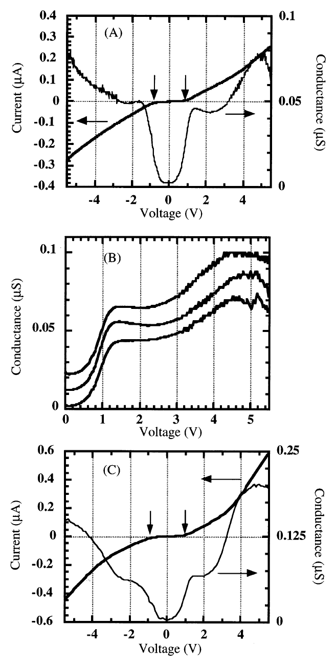One interpretation of the observed gap around zero voltage is as a Coulomb gap. Using the “apparent” Coulomb gap, an experimental capacitance of 1.1 × 10⁻¹⁹ F is obtained. Although the charge transport through the molecule is in principle a many-body effect, as a first step one can estimate the capacitance of the aryl group with a crude model. Using a 4.5 Å metallic sphere bound 2.0 Å from proximal metallic planes with intervening vacuum barriers gives a capacitance of 0.4 × 10⁻¹⁹ F, compared to the experimentally derived 1.1 × 10⁻¹⁹ F. However, a definitive demonstration of Coulomb blockade would require a third gate electrode, which is problematic in the present configuration because of the inability of placing a third proximal probe near the molecule. A second interpretation of the observed gap is due to the mismatch between the contact Fermi level and the LUMO (lowest unoccupied molecular orbital). Preliminary calculations using this interpretation give similar characteristics to the experimentally observed data.25 The reproducibility of the minimum conductance at a consistent value implies that the number of active molecules could be as few as one. A better theoretical understanding of the threshold resistance of this system, either the apparent Coulomb gap derived from the capacitance of a single molecule configuration or the determination of the contact Fermi level-LUMO gap alignment, is needed to compare to the experimental values of ∼22 Mohm and ∼0.7 V, respectively.
The determination of the effective molecule-metal barrier height in the above experiments requires temperature-dependent measurements, which are not possible in the present configuration because of the temperature sensitivity of the MCB junctions. STM has been used to resolve images of single molecules;10 however, these experiments could not give the absolute value of the conductivity because of the involvement of a tunneling gap between the STM tip and the molecule. Reifenberger et al. has developed a method to deduce the zerobias conductivity of an ensemble of molecular wires;11,12 nevertheless the bias range applied across the molecules is small and hence no information concerning current-voltage spectroscopy has been derived. Direct contacting to organic thin films has been executed;16 however, multilayers of the molecular wires and micron scale area of the devices containing a large number of molecules have been used, which complicates the analysis of the transport mechanism of single molecules. Direct contacting to and electrical measurements of a single monolayer of a small number of molecules have not yet been demonstrated.
Here we introduce a novel fabrication technique to directly measure the conduction through a small number of organic molecules. These devices consist of a self-assembled monolayer of conjugated molecular wires sandwiched between top and bottom metallic contacts. This technique guarantees good control over the device area and intrinsic contact stability. Two essential features are included in the process, the first of which is the employment of a nanoscale device area. The area is made to be smaller than the domain size of the SAM and thus the adsorbed organic layer is highly ordered and mostly defect-free. The second feature is that during the deposition of the top contact, several measures are taken to ensure that the deposited metal atoms accumulate at the SAM surface and do not penetrate into the organic layer. These methods also minimize damage to the SAM during the deposition.
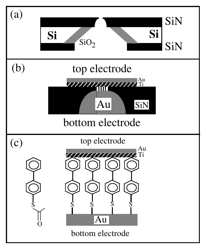A schematic diagram of the device is shown in Figure 5. E-beam lithography followed by plasma etching are used to open a pore in the suspended LPCVD SiN membrane.26 The pore takes a bowl shape with the opening at the upper edge having diameter of ∼30 nm, as shown in Figure 5(a). Gold is evaporated from the bottom side to fill the pore. The typical crystallite size for gold is about 50 nm, and thus the upper surface of gold in the nanopore is probably a single crystallite. The samples are then immediately immersed into a 0.3 millimolar solution of the organic molecules for three days under argon atmosphere. The molecules we use are 4-thioacetylbiphenyl, as shown in Figure 5(c) with a length about 12 Å. It has been demonstrated that under such conditions the functionalized organic molecules would self-assemble onto the gold surface and form a highly ordered monolayer.21 After the formation of the SAM, the samples are taken out of the solution and loaded into a high vacuum chamber of 10−8 torr to deposit the top electrodes. First 10 Å Ti is deposited onto the upper surface of the SAM. This amount of Ti would bond onto the SAM surface and form a continuous film.27 The samples are then maintained at low temperature while 30 Å Ti and 800 Å Au are deposited onto the upper side of the samples, which are thick enough to make the top electrodes continuous and well conducting. This low-temperature deposition helps to minimize the thermal damage to the SAM. A very low deposition rate (∼0.3 Å/s) is also used for the same reason. Detailed schematics of the sandwiched heterostructure are shown in Figures 5(b) and (c). The samples are then allowed to warm up to room temperature slowly (∼24 hr) and ready for measurements. This technique gives us a yield of about 80% working devices. These devices are stable at room temperature and vary only slightly after thermal cycling to ∼50 K.
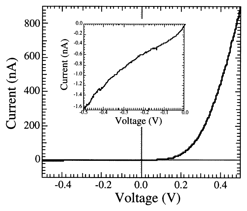Two terminal current (I)-voltage (V) characteristics are measured in the temperature range from room temperature down to 57 K. Figure 6 shows the I-V curves of the device measured at room temperature. Positive bias corresponds to electrons emitted from the Au/Ti top electrode and collected by the bottom Au electrode. I-V characteristics under negative bias are shown in the inset of Figure 6. Prominent rectifying behavior is observed: the current at −1 V bias is about 500 times higher than the current at −1 V bias. While the I-V curve at negative bias is rather linear, the I-V curve at positive bias displays exponential behavior. For different devices, the current magnitude varies slightly due to variation in device area, but the rectifying behavior is always observed. The current is observed to decrease monotonically with temperature under both the positive and negative biases. At 1 V positive bias the current experiences about four orders of magnitude decrease as temperature decreases from room temperature to 57 K, suggesting thermally activated transport mechanism. For thermally activated electron injection from the metal into the SAM, the image force potential causes a lowering of the barrier height and the formula accounting for both thermal activation and image force potential is given by28,29:
I = A e(a√V − qΦ) / kT, where a = (q/2) √( q / 4πεiε0d ) (1)
where A is the effective Richardson constant multiplied by the current injection area, q the electron charge, Φ the thermal emission barrier height, V the bias, k Boltzmann’s constant, T the temperature, εi the relative dielectric constant of the SAM, ε0 the vacuum dielectric constant, and d the thickness of the molecular dielectric film. Figure 7(a) displays the plots of ln(I) versus 1/T for different biases, where the marks represent data points and the lines are least-square fits for each bias. The plots clearly demonstrate that ln(I) is linear with l/T and the slope of the lines is a function of the bias voltage. The standard thermal emission theory predicts:
slope = (a√V − qΦ) / k (2)
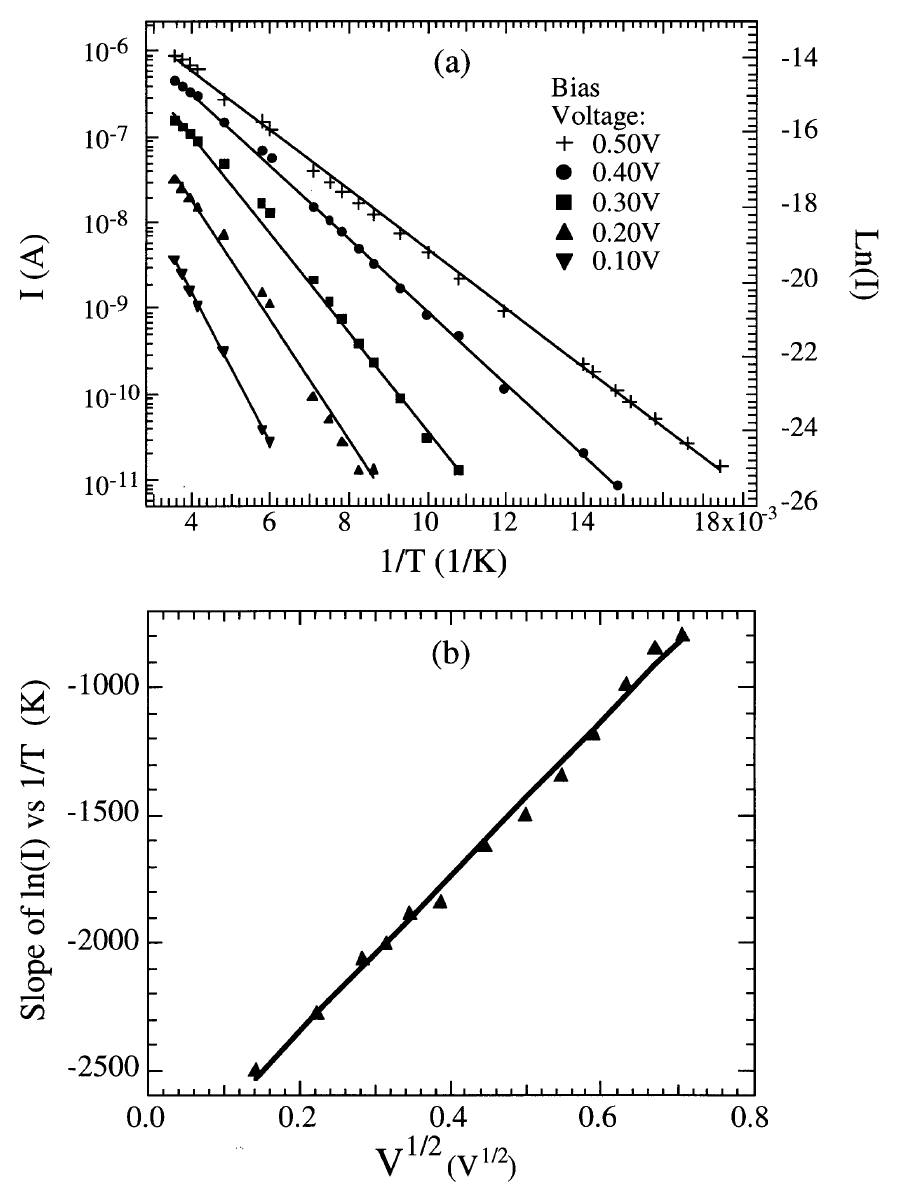One can plot the slope of each line in Figure 7(a) versus V1/2 and derive the constants a and qΦ, as shown in Figure 3(b). The data points are found to lie on a straight line and the least-square fitting yields a value of 0.26 eV for qΦ and 0.263 eV1/2 for a. Given the film thickness of 10 Å as measured from the ellipsometry data, from formula (1), we can further derive the dielectric constant of the SAM to be 4.2.
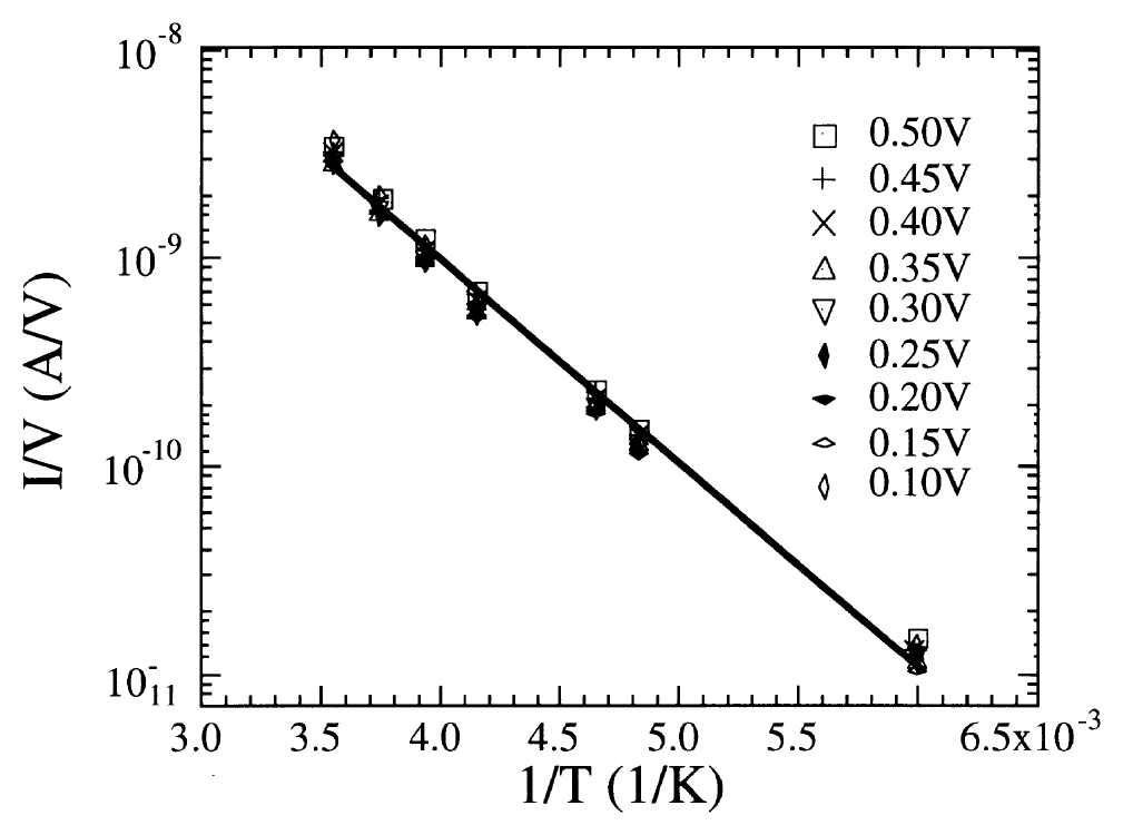
The negative bias corresponds to electrons injected from the Au bottom electrode into the conjugated molecules through the thiolates. The current also decreases with temperature; however, detailed analysis reveals that the data fit into the hopping conduction mechanism, which corresponds to electrons hopping from one site to the neighboring ones.28,30 For different biases, plots of ln(I/V) vs. l/T fall on one line, as shown in Figure 8. The least-square fitting yields a hopping barrier of 0.19 eV. At present it is unclear whether the hopping is related to defects in the SAM, hopping along the molecular wire, or hopping between neighboring molecular wires. Gold is known to have a higher work function than Ti; despite the lack of knowledge about the interface states and the role of sulfur atoms, these results suggest that the barrier for electrons injected from the bottom gold electrode is higher than the barrier for electrons injected from the top Ti electrode. As a result, no prominent thermal emission is observed under negative bias and the current is carried by electrons hopping through the molecular layer instead of electrons thermally activated over the Au/SAM barrier.
Conclusion
We have demonstrated new fabrication techniques to study the transport mechanism of organic molecular wires. MCBs and nanoscale fabrication with special metal deposition techniques are employed to provide metallic contacts to the self-assembled monolayer of a small number of conjugated molecular wires. In one case, we have measured the conductivity of a single molecule. In another, because of the asymmetry in the heterostructure, prominent rectifying behavior is observed in the I-V characteristics. These methods can be easily adapted to other molecular wire systems for determination of transport mechanism and band alignment.
Acknowledgments
We acknowledge DARPA for financial support. We thank M. Rooks and CNF for their help.
References
- Reed, M.A. et al. 1988. Observation of discrete electronic states in a zero-dimensional semiconductor nanostructures. Phys. Rev. Lett. 60: 535–538.
- Meirav, U. et al. 1990. Single electron charging and periodic conductance resonances in GaAs nanostructures. Phys. Rev. Lett. 65: 771–774.
- Dellow, M. et al. 1992. Resonant tunneling through the bound states of a single donor atom in a quantum well. Phys. Rev. Lett. 68: 1754–1757.
- Kouwenhoven, L.P. et al. 1991. Single electron charging effects in semiconductor quantum dots. Z. Phys. B 85: 367–373.
- Tewordt, M. et al. 1992. Resonant tunneling in an AlGaAs/GaAs quantum dot as a function of magnetic field. Phys. Rev. B 46: 3948–3952.
- Su, B. et al. 1992. Single-electron tunneling in nanometer-scale double-barrier heterostructure devices. Phys. Rev. Lett. 46: 7644–7647.
- Klein, D.L. et al. 1996. An approach to electrical studies of single nanocrystals. Appl. Phys. Lett. 68: 2574–2576.
- Ralph, D.C. et al. 1997. Gate-voltage studies of discrete electronic states in aluminum nanoparticles. Phys. Rev. Lett. 78: 4087–4090.
- Grabert, H. et al. 1991. Single Electron Tunneling. Plenum. New York.
- Bumm, L.A. et al. 1996. Are single molecular wires conducting. Science 271: 1705–1707.
- Dorogi, M. et al. 1995. Room temperature Coulomb blockade from a self-assembled molecular nanostructure. Phys. Rev. B 52: 9071–9077.
- Andres, R.P. et al. 1996. Coulomb staircase at room temperature in a self-assembled molecular nanostructure. Science 272: 1323–1325.
- Crommie, M.F., C.P. Lutz & D.M. Eigler. 1993. Spectroscopy of a single adsorbed atom. Phys. Rev. B 48: 2851–2854.
- Joachim, C. et al. 1995. Electronic transparence of a single C60 molecule. Phys. Rev. Lett. 74: 2102–2105.
- Yazdani, A. et al. 1996. Off-resonance conduction through atomic wires. Science 272: 1921–1924.
- Fischer, C.M. et al. 1995. Microstructured gold/Langmuir-Blodgett film/gold tunneling junctions. Appl. Phys. Lett. 66: 3331–3333.
- Grabert, H. 1991. Single charge tunneling: A brief introduction. Z. Phys. B 85: 319–325.
- Nejoh, H. 1991. Incremental charging of a molecule at room temperature using the scanning tunneling microscope. Nature 353: 640–642.
- Muller, C. J. et al. 1992. Experimental observation of the transition from weak link to tunnel junction. Physica C 191: 485–504.
- Muller, C. J. et al. 1996. Quantization effects in the conductance of metallic contacts at room temperature. Phys. Rev. B 53: 1022–1025 and references therein.
- Tour, J.M. et al. 1995. Self-assembled monolayers and multilayers of conjugated thiols, α,ω-dithiol, and thiolacetyl-containing adsorbates. understanding attachments between potential molecular wires and gold surfaces. J. Am. Chem. Soc. 117: 9529.
- Zhou, C. et al. 1995. Microfabrication of a mechanically controllable break junction in silicon. Appl. Phys. Lett. 67: 1160–1162.
- Mujica, V. et al. 1996. Current-voltage characteristics of molecular wires: Eigenvalue staircase, Coulomb blockade and rectification. J. Chem. Phys. 104: 7296–7305.
- Samanta, M.P. et al. 1996. Electronic conduction through organic molecules. Phys. Rev. B 53: R7626–R7629.
- Datta, S. Unpublished material.
- Ralls, K.S. et al. 1989. Fabrication of thin-film metal nanobridges. Appl. Phys. Lett. 55: 2459–2461.
- Konstadinidis, K. et al. 1995. An in-situ X-ray photoelectron study of the interaction between vapor-deposited Ti atoms and functional groups at the surfaces of self-assembled monolayers. Surf. Sci. 338: 300.
- Sze, S.M. 1981. Physics of Semiconductor Devices, 2nd ed.: 403. Wiley. New York.
- Lamb, D.R. 1967. Electrical Conduction Mechanisms in Thin Insulating Films: 47. Methuen. London.
- Okada, K. et al. 1997. Electrical stress-induced variable range hopping conduction in ultrathin silicon dioxide. Appl. Phys. Lett. 70: 351–353.
Provenance
- Shelf
- Reference Library
- File
- database/content/pages/reed-1998-molecular-junctions.json
- Rights
- Reed M.A., Zhou C., Deshpande M.R., Muller C.J., Burgin T.P., Jones L. II and Tour J.M., 'The Electrical Measurement of Molecular Junctions', Annals of the New York Academy of Sciences 852 (1998) 133–144, doi:10.1111/j.1749-6632.1998.tb09868.x. © 1998 The New York Academy of Sciences. Transcribed from a copy of the printed pages for study and reference; figures cropped from the same pages. The note at the head of the page is the archive's.