

patent · US4151005A
Radiation hardened semiconductor photovoltaic generator
24 April 1979
Text
Page 1bibliographic recordscan →
United States Patent (19)
Strebkov et al.
(54) RADATION HARDENED
SEMCONDUCTORPHOTOVOLTAC
GENERATOR
(76 Inventors: Dmitry S. Strebkov, Kirovogradsky proezd, 3, korpus 1, kv. 17; Vitaly V.
Zadde, poselok Severny, 9, linia, 3, kv. 120; Vadim A. Unishkov, ulitsa
Tatyana A. Litsenko, ulitsa
Trubnaya, 11, kv. 12, all of Moscow,
U.S.S.R.; Arkady P. Landsman, deceased, late of Moscow, U.S.S.R.;
by Olga V. Nekljudova, administra trix, Rizhsky proezd, 3, kv. 140,
Moscow, U.S.S.R.
Int. Cl. ............................................. HOL 31/06
3,018,313 1/1962 Gattone ................................ 136/89 3,780,722 12/1973 Swet ............. ... 126/270
3,928,073 12/1975 Besson et al. .............. ... 136/89 3,985,116 10/1976 Kapany ........ ... 126/270 4,021,267 5/1977 Dettling ........... ... 136/89 PC 4,042,417 8/1977 Kaplow et al. ................. 136/89 PC Primary Examiner-John H. Mack
Assistant Examiner-Aaron Weisstuch
Attorney, Agent, or Firm-Lackenbach, Lilling & Siegel
pg, 1 The semiconductor photovoltaic generator com prises one or several photovoltaic converters, each of which is provided with a rectifying barrier, which sepa rates its base region from the inversion region, and with at least two current collector contacts, one of which being connected to the base region and the other being connected to the inversion region. The operating sur face of the semiconductor photovoltaic generator is covered with a protection layer which receives the direct incident radiation and passes the photoactive part of the spectrum thereof to the operating surface of the semiconductor photovoltaic generator. The protection layer comprises elements transparent to the photoactive part of the incident radiation and intermediate metal layers to protect the photovoltaic converter material from the radiation effects which are liable to damage the semiconductor and lower the performance of the semiconductor photovoltaic generator.
18 Claims, 20 Drawing Figures
Drawings
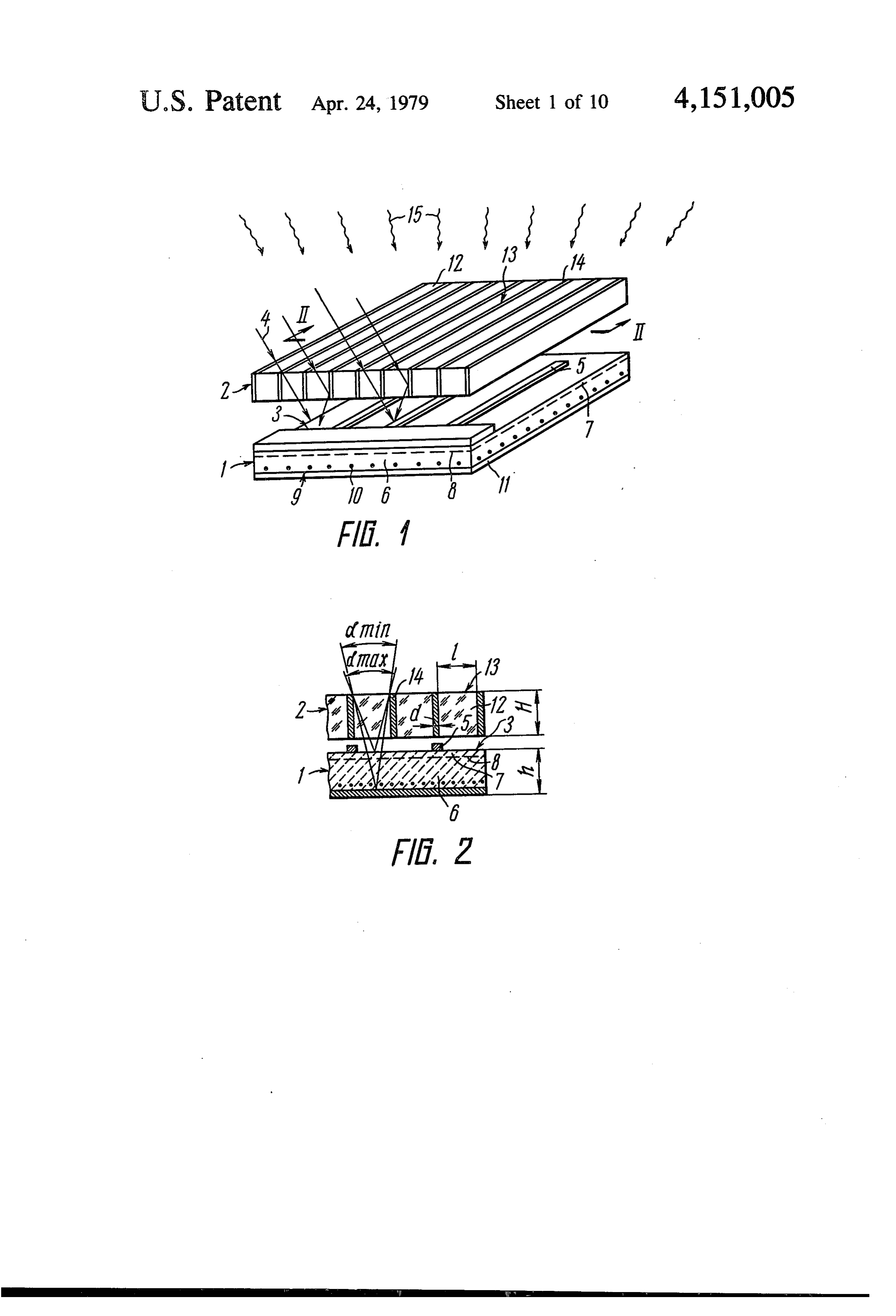
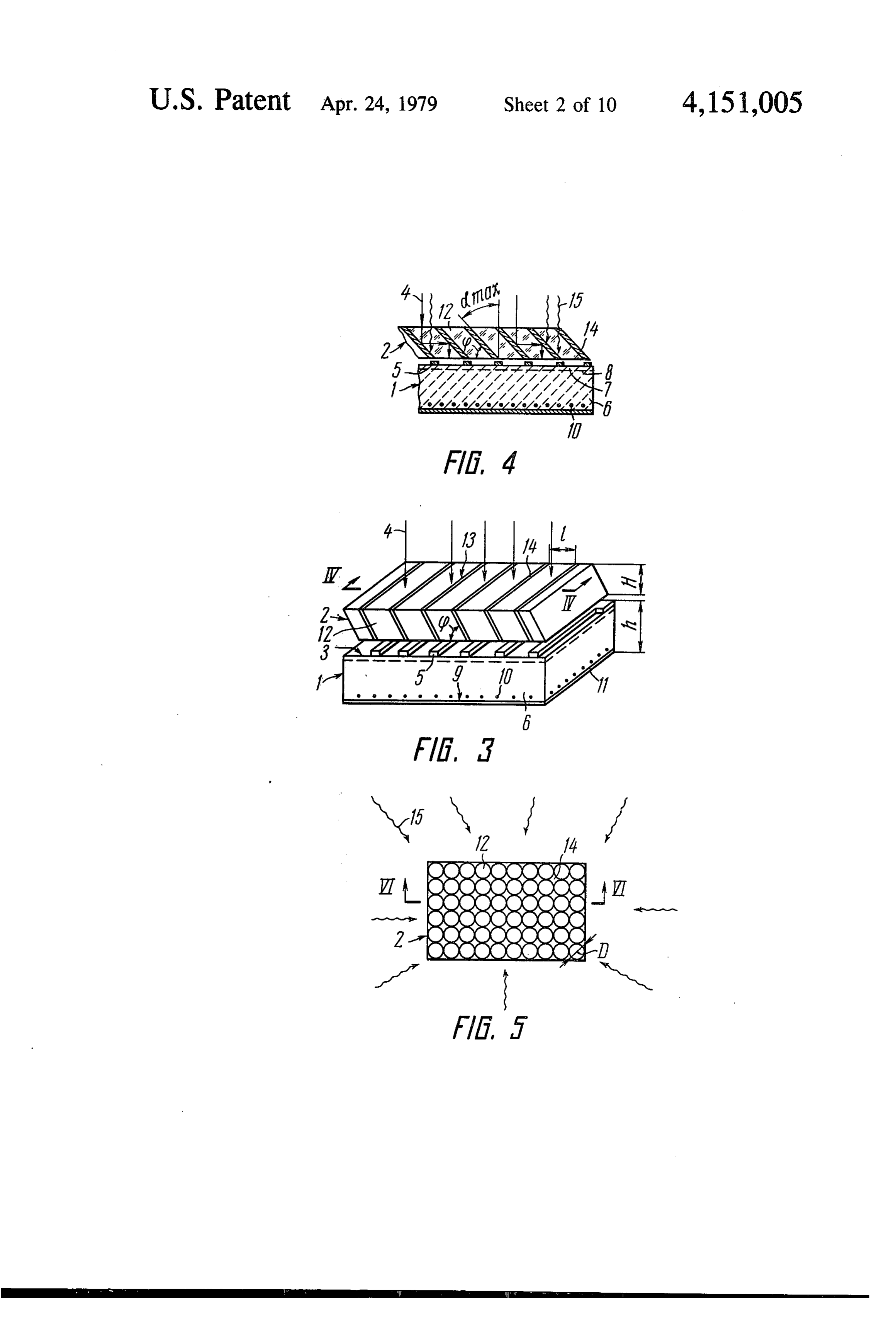
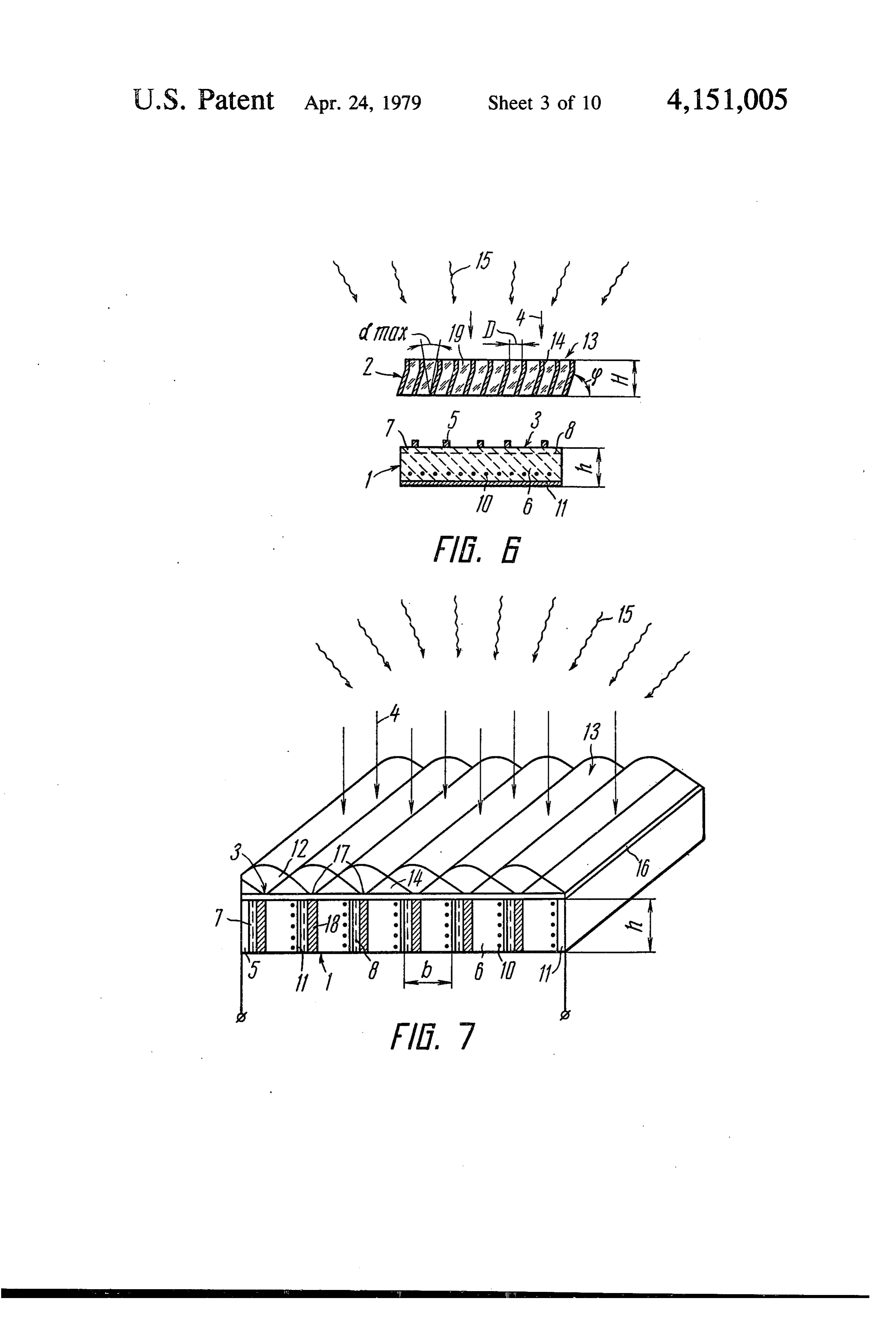
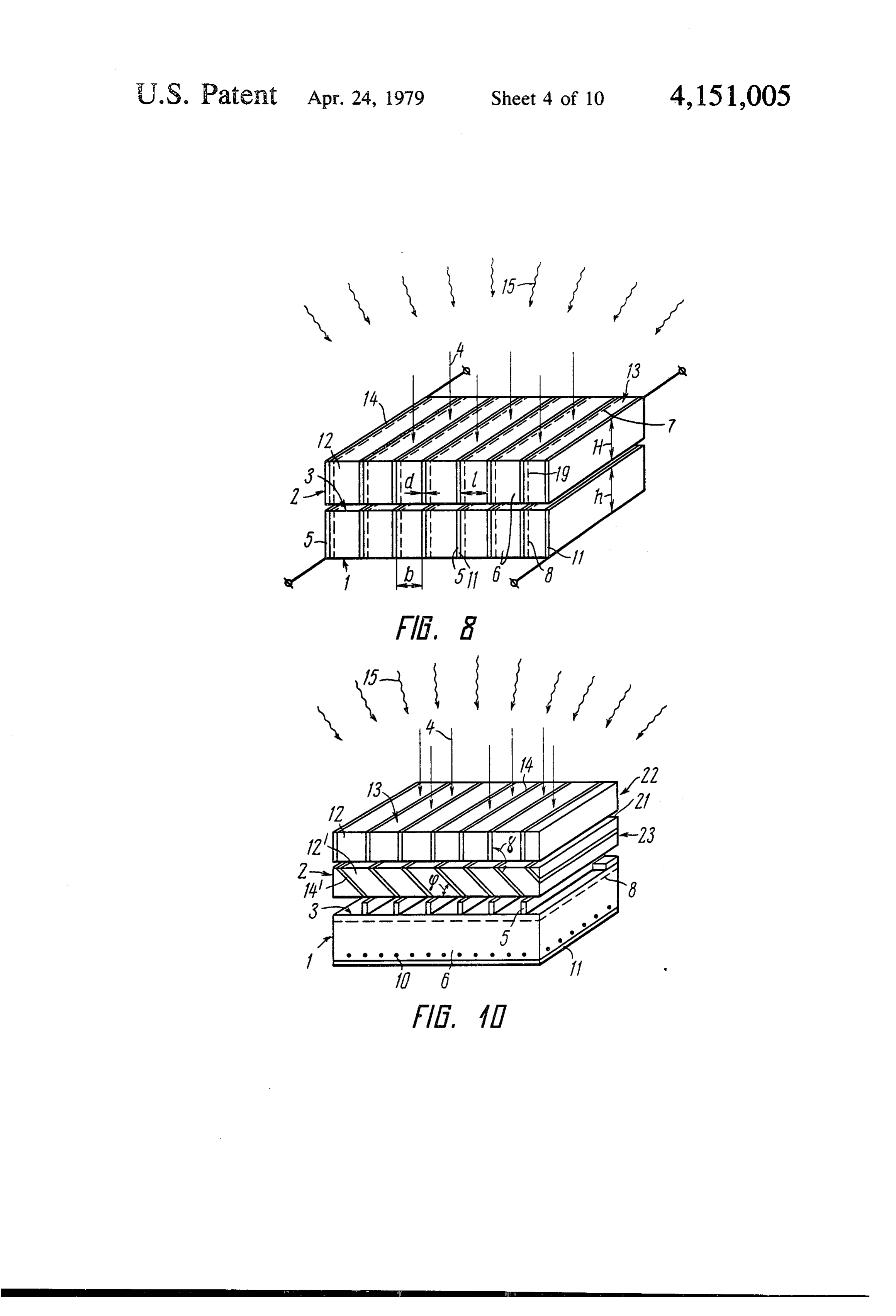
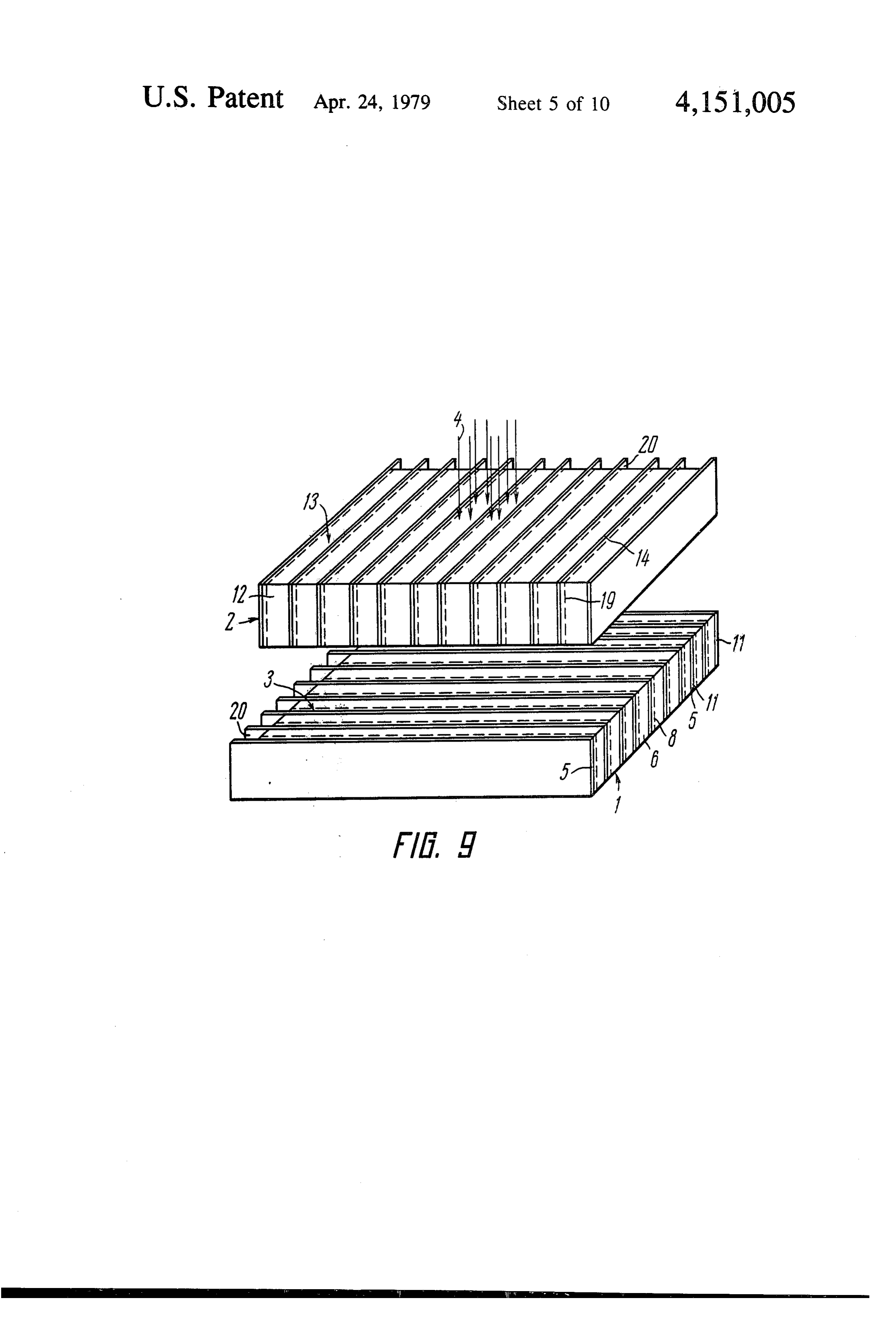
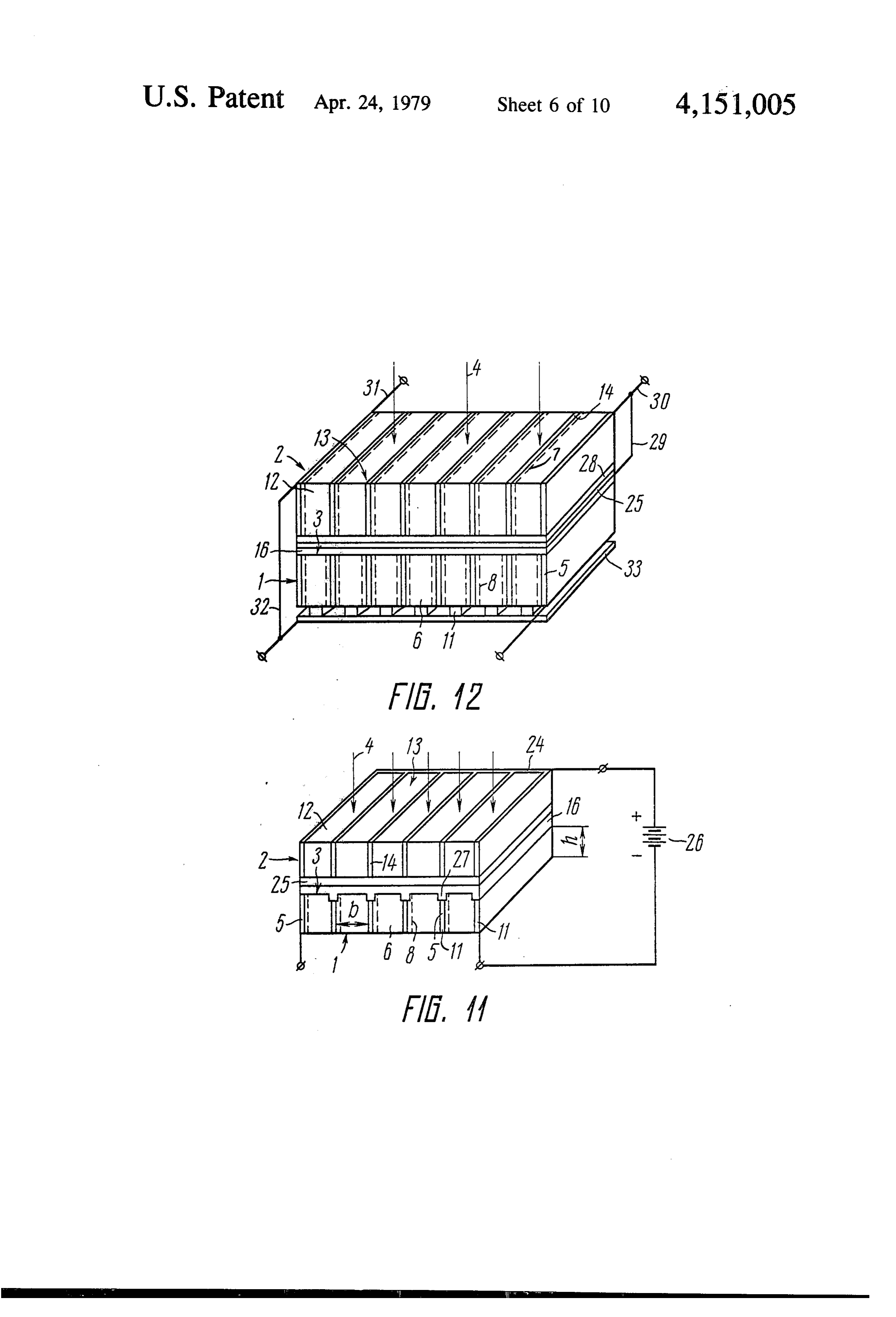
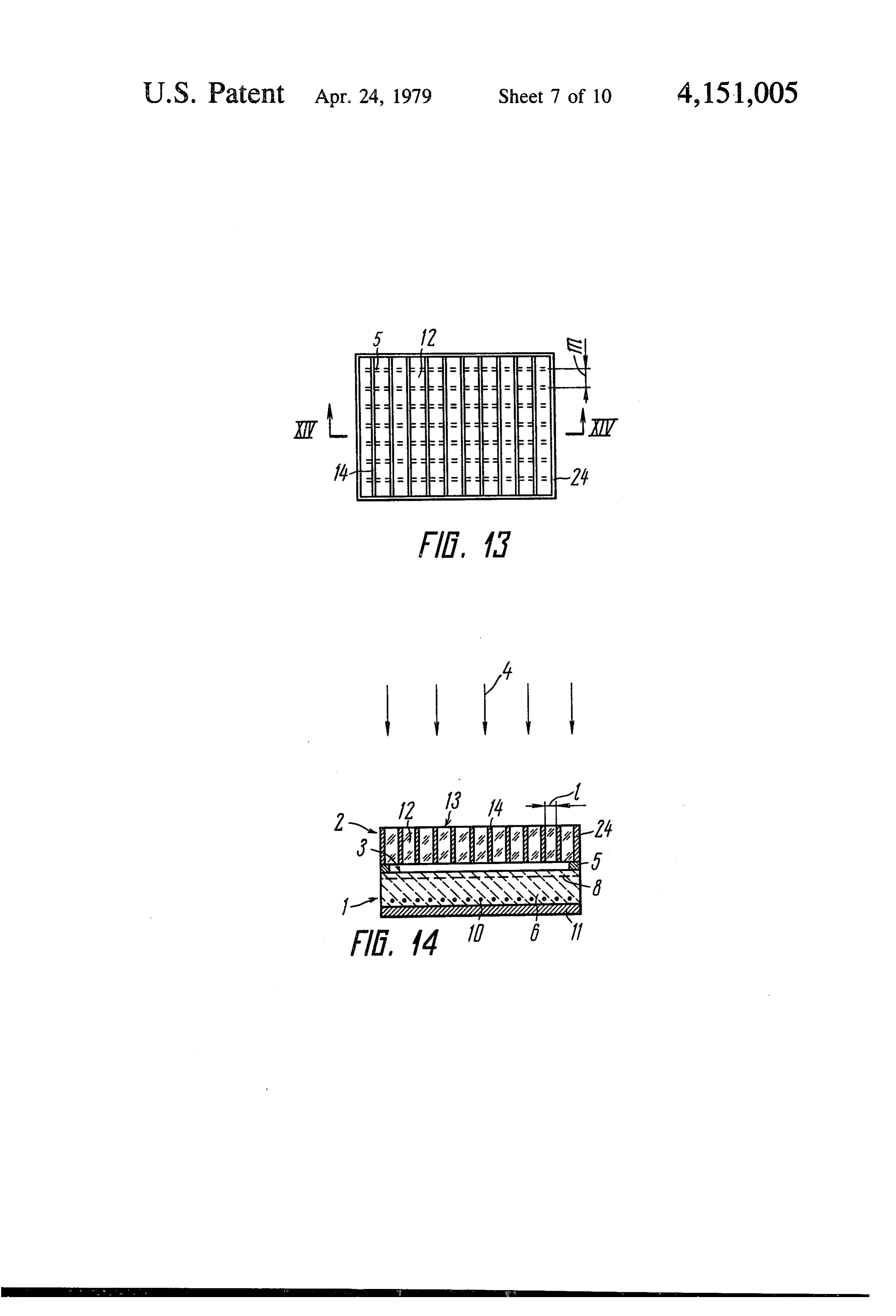
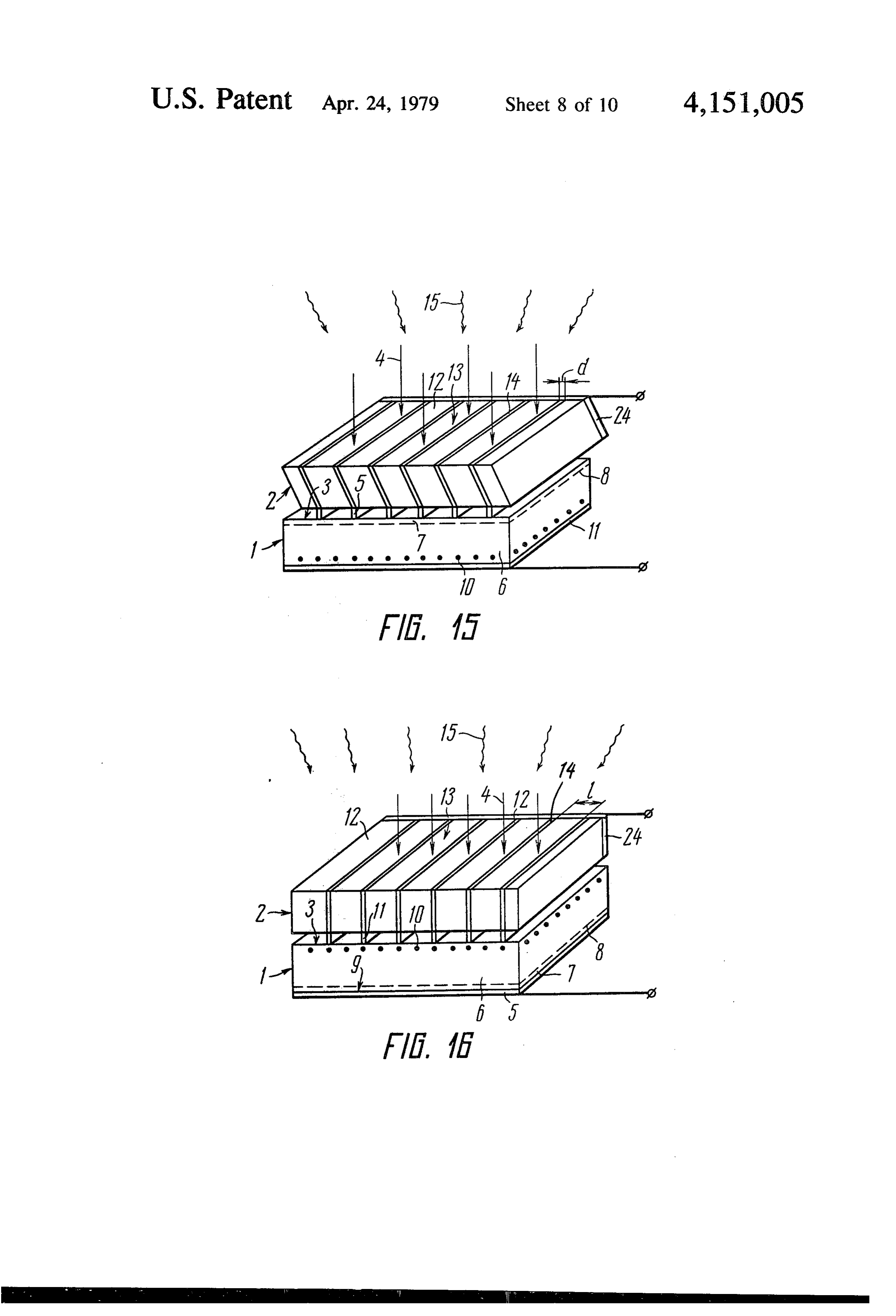
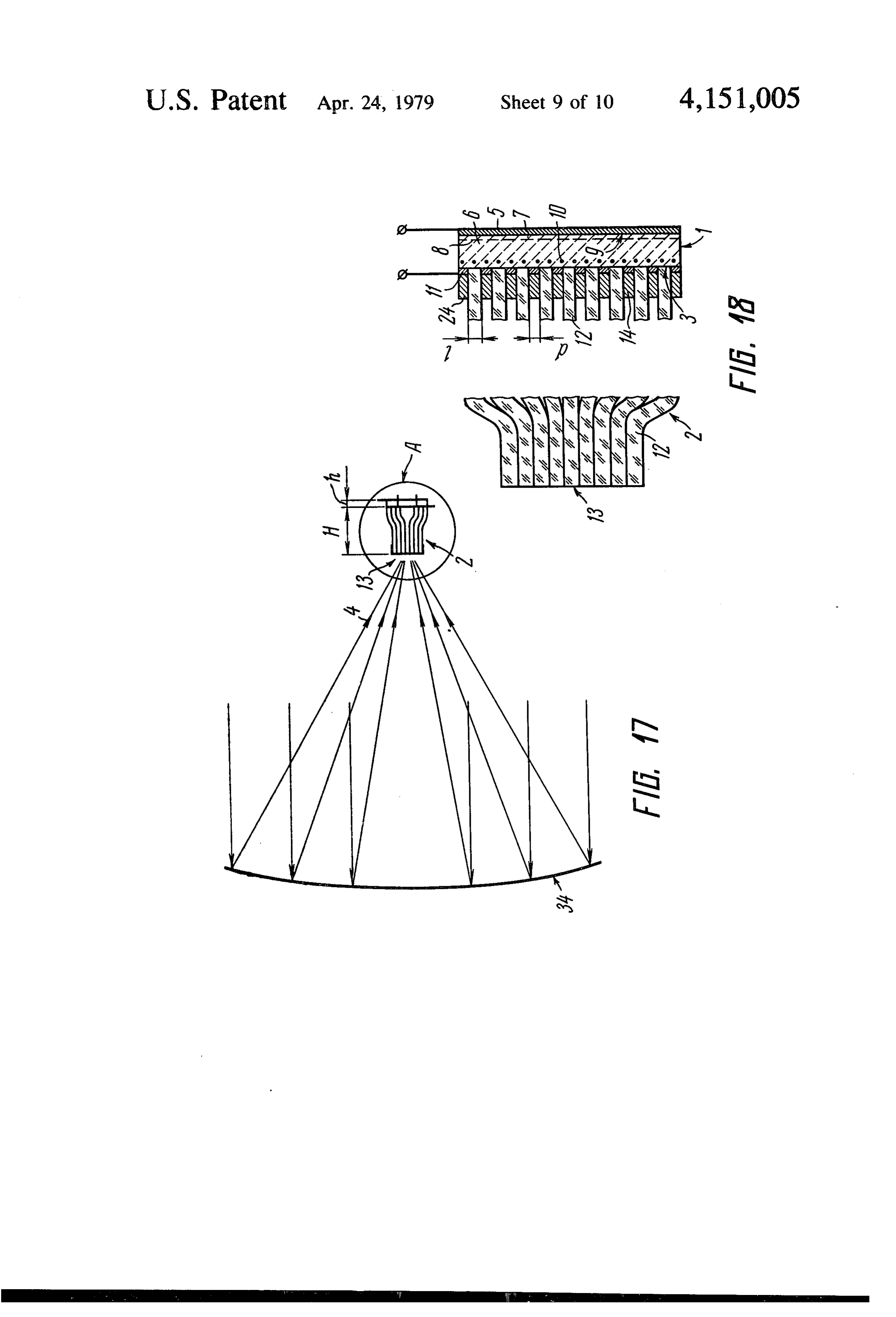
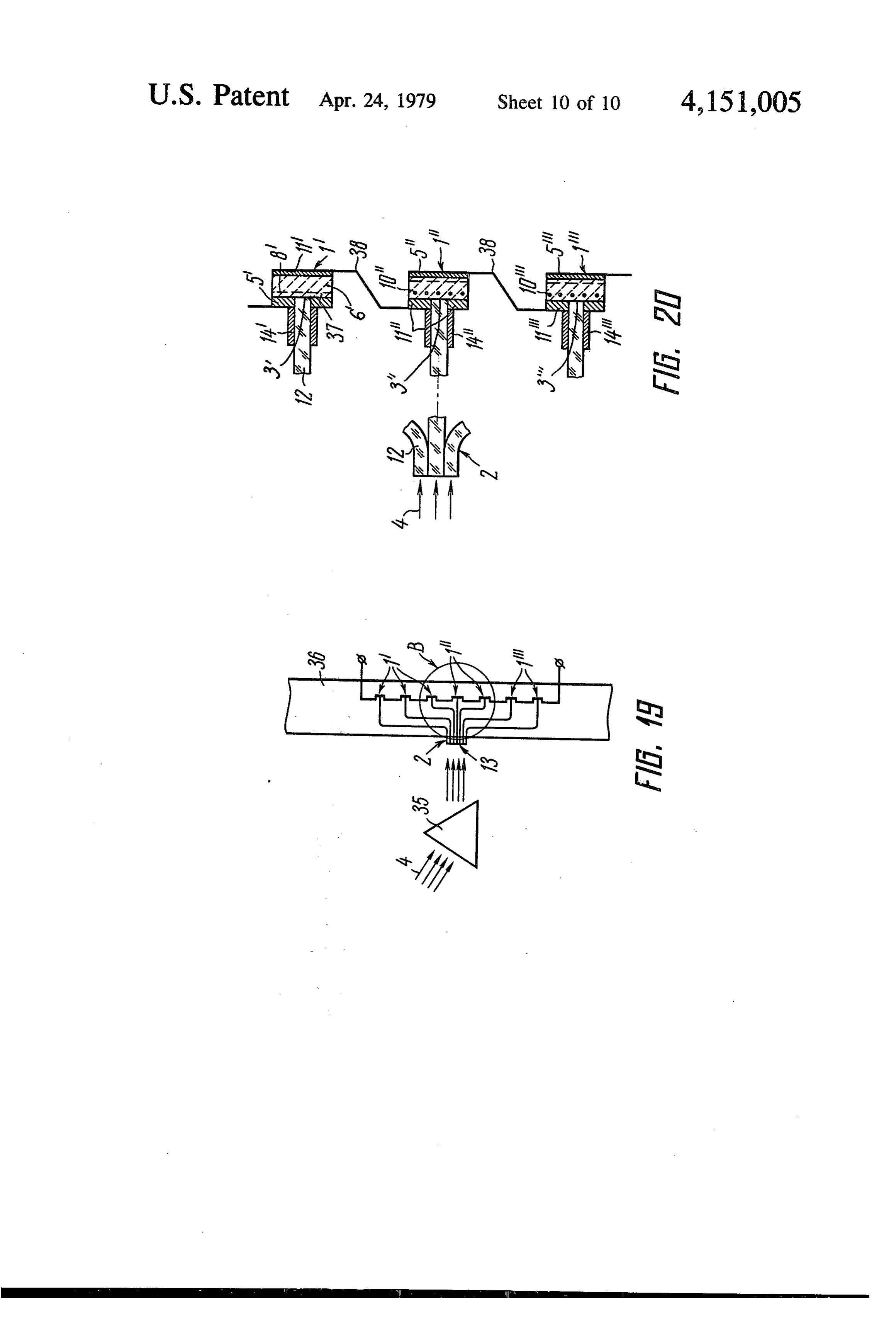
FIG. 19 is a drawing of still another design version of to the photovoltaic converter 1 with the use of a thin the semiconductor photovoltaic generator according to coat of glue.
Page 2drawing sheetscan →
Page 3drawing sheetscan →
Page 4drawing sheetscan →
Page 5drawing sheetscan →
Page 6drawing sheetscan →
Page 7drawing sheetscan →
Page 8drawing sheetscan →
Page 9drawing sheetscan →
Page 10drawing sheetscan →
Page 11drawing sheetscan →
Page 12scan →
Reduction of the gaps between the current collector
RADATION HARDENED SEMICONDUCTOR contacts and an increase of their widths will result in a PHOTOVOLTAC GENERATOR drop of the series resistance and, due to the fact that the operating surface of the semiconductor photovoltaic
The invention relates to devices designed to convert 5 generator is shadowed by the current collector contacts radiation energy into electric energy and in particular to to a higher degree a decrease in the efficiency of the semiconductor photovoltaic generators that are used to generator.
produce solar cell arrays for space vehicles and for Also known in the art is a semiconductor photovol ground-based solar power stations. taic generator made as a solid-state array of microminia The prior art includes a semiconductor photovoltaic 10 ture photovoltaic converters, generator comprising photovoltaic converters intercon These photovoltaic converters are designed as micro nected electrically. miniature parallepipeds combined in a solid-state array The photovoltaic converter is made as a plate of by metal current collector contacts which are arranged semiconductor material in which a p-n junction is pro along all the side facets of said microminiature paral duced by means of doping, the junction serving as a 15 lepipeds. The side facets are tilted by a certain angle rectifying barrier which separates current carriers in with respect to the operating surface of the semiconduc accordance with the polarity of their charges. tor photovoltaic generator. The p-n junction planes are Thus, the p-n junction separates the base region hav located on one, two, three, four or five parallepiped ing one type of conduction due to current carriers that facets while the width of each microminiature paral form the majority in the base region from the inversion 20 lepiped base is about equal to the diffusion length L of region having the opposite type of conduction due to the minority current carriers in the base region. current carriers that form the majority in the inversion The resistance of the current collector contacts of region but belong to the minority in the base region. such semiconductor photovoltaic generators is negligi The base region also comprises an isotype junction. In a ble (about several thousands of Ohms). However, the p-type base region this junction has a p-pit structure, 25 spread resistance that exists in the doped layer located while in an n-type base region the isotype junction has in the immediate vicinity of the operating surface will an n-n structure. lower the efficiency of such semiconductor photovol Current collector contacts are connected to the base taic generators when the radiation power exceeds 50 region and to the inversion region which in this case is W/cm2.
obtained by means of doping, i.e. it represents a doped 30 Besides, the above semiconductor photovoltaic gen layer. The thickness of the base region is commensurate erator made as a solid-state array has a high leakage with the diffusion length L of the minority current current flowing through the p-n junction. If there is no carriers in the base region. The thickness of the inver p-n junction near the operating surface and the base sion region (or the doped layer) is hundreds of times as region constitutes the major part thereof, the current small as the thickness of the base region. The p-n junc 35 losses will increase due to the process of minority cur tion is located near the operating surface of the semi rent carrier recombination in the base region on the conductor photovoltaic generator which receives the surface of the microminiature photovoltaic converter incident radiation. The p-n junction is separated from facets that are free of the p-n junction. the operating surface by the doped layer and the isotype The prior art also includes a photovoltaic generator junction is shifted from the operating surface of the made of photovoltaic converters which are connected semiconductor photovoltaic generator and located electrically and have p-n junctions and isotype junc close to its opposite rear surface. tions in the base region. The isotype junctions are lo The current collector contacts connected to the cated in the immediate vicinity of the operating surface doped region that comes out onto the operating surface of the semiconductor photovoltaic generator and the of the semiconductor photovoltaic generator have a 45 p-n junctions are removed from the operating surface comb-like structure. They occupy no more that 10% of by a distance which does not exceed the diffusion length the operating surface area of the semiconductor photo L of the minority current carriers in the base region. voltaic generator. The current collector contact con In such a semiconductor photovoltaic generator low nected to the base region is made as a thin metal plate power losses caused by the spread resistance in the base occupying the whole of the rear surface of the semicon 50 region and by the resistance of the current collector ductor photovoltaic generator. Therefore, such genera contacts will be obtained only when at least two linear tors have but one operating surface. Their series resis dimensions of a microminiature photovoltaic converter tance for the operating surface area including the area are commensurate with the diffusion length L of the occupied by the current collector contact is compara minority current carriers in the base region. However, tively high (in the order of several tenths of Ohm/cm2). 55 the surface areas of the base region of such photovoltaic The major components of the series resistance are the converters that are located between the p-n junction spread resistance in the thin doped region and the base and the isotype junction considerably exceed the area of region resistance for the current flowing along the thin the p-n junction in size and the recombination rate of narrow bands of the current collector contact on the carriers on them is quite high, which prevents the cur operation surface. A high value of the series resistance 60 rent carriers generated by the incident light from reach lowers the efficiency of the generator when the incident ing the p-n junction and, thereby causes excessive cur energy power exceeds 0.5 W/cm2. rent and voltage losses.
With an increase of the depth where the p-n junction Known also is a semiconductor photovoltaic genera is located, the spectral sensitivity of such generators is tor whose operating surface is provided with a protec lowered while if this junction is brought out closer to 65 tion cover made of a transparent material, such as the surface, there will be an increase of the spread resis methyl methacrylate, which seals the photovoltaic con tance in the doped layer and a growth of the leakage verters hermetically and guards them from the damag current flowing through the p-n junction. ing effects of the environment. The protection cover 13 may also form an optical lens to focus the radiation that The object of the present invention is to provide a passes through it. semiconductor photovoltaic generator having an in A common drawback of all the above semiconductor creased resistance to damaging radiation while preserv photovoltaic generators is that their efficiency will drop ing the same size and weight. at an accelerated pace under the effect of damaging Another object of the present invention is to reduce radiation due, for instance, to cosmic rays, radiation the series resistance of the semiconductor photovoltaic belts of the earth and thermonuclear reactions. generator and to raise its efficiency irrespective of the When a semiconductor photovoltaic generator re radiation energy concentration, including concentra ceives a sufficiently high dose of accelerated charged tions exceeding 1 W/cm2.
particles that form damaging radiation, the amount of 10 Still another object of the invention is to increase the the current or voltage produced by it will drop due to current and voltage sensitivity of the semiconductor radiation caused defects in the semiconductor structure photovoltaic generator.
and to the reduction of the diffusion length L of the The above objects are achieved by means of a semi minority current carriers. conductor photovoltaic generator comprising: at least The radiation resistance of the known semiconductor 15 one photovoltaic converter whose rectifying barrier photovoltaic generator designs is achieved by means of introducing certain dopants of the required concentra separates due to the the base region having one type of conduction majority current carriers for the base region tion into the base region. It is known that the radiation from the inversion region having the opposite type of resistance of a base region made of a p-type silicon will conduction due to the minority current carriers for the be several times as high as that of a base region made of 20 a n-type silicon. Besides, the lower the doping concen base region: at least two current collector contacts one tration in the base region the higher the radiation resis of which being connected to the base region and the tace. However, it is impossible for all known semicon other being connected to the inversion region; and a ductor photovoltaic generators to operate for a long protection cover receiving the incident radiation and time without additional protection against the damag 25 located at least on one operating surface of the semicon ing radiation. Such protection can only be provided ductor photovoltaic generator receiving the incident with the use of protection covers of a considerable radiation that has passed through the protection cover. thickness (about 1 mm) placed onto the operating sur According to the invention, said protection cover is face of a semiconductor photovoltaic generator. made as a set of elements touching each other at least It is quite evident that the use of thick glass, quartz or 30 near the receiving surface of the protection cover and sapphire protection layers as well as the provision of allows at least a part of the radiation spectrum which is excessive power reserves in semiconductor photovol photoactive for the given photovoltaic converter to taic generators designed to serve as power supplies on pass to the operating surface of the semiconductor pho board space vehicles makes them cumbersome and tovoltaic generator. Intermediate layers which absorb heavy and decreases their weight characteristics. 35 the radiation damaging the photovoltaic converter are The prior art includes a method of raising the ability located between adjacent elements.
of glass to absorb the damaging radiation. It consists of Preferably the protection cover in the semiconductor doping the glass with materials of a heavy atomic photovoltaic generator is made as an array of micromin weight (for instance, lanthanides). However, high con iature elements arranged in rows as a single layer, the centrations of such dopants reduces the glass optical thickness of the protection cover being commensurate properties. with the linear dimension of the photovoltaic converter Known in the art is a semiconductor photovoltaic as measured in the direction orthogonal to the operating generator comprising a set of photovoltaic converters surface of the semiconductor photovoltaic generator. arranged in such a manner that their thin inversion Conveniently the protection cover elements are made region appears at the operating surface of the semicon 45 as parallepipeds whose linear dimension as measured in ductor photovoltaic generator. Connected to the base the direction parallel to the operating surface of the and to the inversion regions are current collector metal semiconductor photovoltaic generator is commensurate contacts made in the inversion region in the form of a with the diffusion length L of the minority current comb. The operating surface is covered with a protec cariers in the base region, while the side facets limiting tion layer made as a glass plate bearing metallization 50 said linear dimension are tilted by an angle O'<d (180° bands in areas which correspond to those where current with respect to the operating surface and the adjacent collector contacts are located on the operating surface . side facets are interconnected and fastened to one an of the semiconductor photovoltaic generator. The pro tection layer is soldered to the generator by said metalli other through intermediate layers. Preferably, the protection cover elements are made as zation bands. 55
This design of a semicnductor photovoltaic generator cylinders the base diameter of which is commensurate with the diffusion length L of the minority current does not provide for increased radiation resistance since carriers in the base region, the cylinders being tilted by the absorption properties of a protection layer depends only on the thickness of the glass plate. Besides, the an angle 0<db< 180 with respect to the operating problem of finding an optimum ratio between the area surface of the semiconductor photovoltaic generator, occupied by the current collector contacts on the oper interconnected and fastened to one another through ating surface and the value of the series resistance of the intermediate layers.
generator is not solved either since an increase of the Conveniently the intermediate layers of the protec current collector contact area will result not only in the tion cover are made of a current-conducting material reduction of the series resistance but also in the shadow 65 and are connected electrically to the current collector ing of the operation surface, which does not allow high contacts located on the operating surface of the semi efficiencies especially in cases of high radiation powers conductor photovoltaic generator and coupled with a exceeding 1 W/cm2. common current-carrying bus.
Page 14scan →
It is expedient that the base region thickness of the the protection cover elements made of a semiconductor photovoltaic converter be less than the diffusion length material being arranged in series in an electric network, L of the minority current carriers in the base region. one lead of which being connected to one of the current In an arrangement which is often convenient, all the collector contacts of the photovoltaic converter and the intermediate layers of the protection cover touch the other lead being connected to the current conducting current collector contacts on the whole of the external layer.
surface of the latter protruding over the operating sur A semiconductor photovoltaic generator designed face of the semiconductor photovoltaic generator. according to the present invention exhibits an increased Conveniently, at least a part of the protection cover resistance to the damaging radiation while preserving elements are made of the semiconductor material form 10 the same size and weight, an increased efficiency even ing photovoltaic converters. in case of higher concentrations of photoactive radia It is expedient that the semiconductor photovoltaic tion and an increased current and volt age sensitivity. converters, having separate current collector contacts, These and other objects of the invention will become the converters being insulated electrically from each apparent from the following detailed description of its other and located in a row, the linear dimension of said 15 embodiments taken as examples together with the ac photovoltaic converters as measured along the row in companying drawings in which the plane of operation surface being commensurate with FIG. 1 is a perspective view of the semiconductor the diffusion length L of the minority carriers in the photovoltaic generator according to the invention; base region and the direction of the protection cover FIG. 2 is a cross sectional view taken along the line element rows being orthogonal to the direction of the 20 II-II in FIG. 1 according to the invention, photovoltaic converter rows. FIG. 3 is a perspective view of another embodiment In an arrangement which is often convenient, the of the semiconductor photovoltaic generator according protection cover elements are made as optical concen to the invention, trators focusing the incident radiation into a focal spot FIG. 4 is a cross sectional view taken along the line so that the absorption zone of the radiation focused into 25 IV-IV in FIG.3 according to the invention, the focal spot is located within the base region of the FIG. 5 is a top view of another embodiment of the photovoltaic converter and shifted from the rectifying semiconductor photovoltaic generator according to the barrier by a distance smaller than the diffusion length L invention, of the minority current carriers in the base region. FIG. 6 is a cross sectional view taken along the line It is expedient that the protection cover of the semi 30 VI-VI in FIG. 5 according to the invention, conductor photovoltaic generator comprises two arrays FIG. 7 is a perspective view of still another embodi of elements, the arrays being superimposed on each ment of the semiconductor photovoltaic generator ac other so that the intermediate layers of one array are cording to the invention, located at an angle with respect to those of the other FIG. 8 is a perspective view of a design version of the array. 35 semiconductor photovoltaic generator having a protec Preferably, the parts of the protection cover elements tion cover made as an array of semiconductor elements facing the operating surface of the semiconductor pho according to the invention, tovoltaic generator are arranged so as to diverge in a FIG. 9 is a perspective view of still another embodi fan-like manner and the intermediate layers made of a ment of the semiconductor photovoltaic generator de current conducting material are connected electrically sign having a protection cover made as an array of to the current collector contacts located on the operat semiconductor elements according to the invention, ing surface. FIG. 10 is a perspective view of the semiconductor It is expedient that every element of the protection photovoltaic generator with a two-layer protection cover operates in conjunction with a separate photovol cover according to the invention, taic converter. 45 FIG. 11 is a perspective view of still another embodi Conveniently, the semiconductor photovoltaic gen ment of the semiconductor photovoltaic generator ac erator comprises phtovoltaic converters whose base cording to the invention, regions serve as a section of the operating surface of the FIG. 12 is a perspective view of still another embodi semiconductor photovoltaic generator covered with a ment of the semiconductor photovoltaic generator ac dielectric, the intermediate layers of the protection 50 cording to the invention, cover being made of a current conducting material and FIG. 13 is a top view showing one of the possible being brought out to a common current carying bus design versions of the semiconductor photovoltaic gen connected to one pole of a DC power supply, the other erator according to the invention, pole of which being connected to the current collector FIG. 14 is a cross sectional view taken along the line contact on the operating surface of the semiconductor 55 XIV-XIV of the design version shown in FIG. 13 photovoltaic generator, and a layer of a current con according to the invention, ducting material being provided between the dielectric FIG. 15 is a perspective view of still another of the layer and the protection cover, said layer being con semiconductor photovoltaic generator according to the nected electrically to the intermediate layer. invention,
It is expedient that the semiconductor photovoltaic FIG. 16 is a perspective view of still another of the generator comprises photovoltaic converters the base semiconductor photovoltaic generator according to the region of which serves as sections of the operating sur invention, face of the semiconductor photovoltaic generator, said FIG. 17 is a drawing of the semiconductor photovol sections being covered with a dielectric, the protection taic generator provided with a sun radiation concentra cover surface facing the operation surface of the semi 65 tor according to the invention, conductor photovoltaic generator being also coated FIG. 18 is an enlarged view of the longitudinal sec with a dielectric and a layer of a current conducting tion A of the design shown in FIG. 17 according to the material being provided between said dielectric layers, invention,
Page 15scan →
FIG. 19 is a drawing of still another design version of to the photovoltaic converter 1 with the use of a thin the semiconductor photovoltaic generator according to coat of glue.
the invention, and The basic semiconductor material to serve as the base FIG. 20 is an enlarged view of the longitudinal sec region 6 of the photovoltaic converter 1 is selected from tion B of a part of the semiconductor photovoltaic gen 5 substances having the greatest diffusion length of mi erator shown in FIG. 19 according to the invention. nority current carriers. The minority carrier diffusion Presented in FIG. 1 is a semiconductor photovoltaic length for silicon, for instance, is about 100 am. In order generator comprising a photovoltaic converter 1 and a to ensure that all the photoexcited minority current protection cover 2. To simplify the discussion of the carriers are collected at the p-n junction 8, the thickness design, the protection cover 2 and the photovoltaic 10 of the base region 6 should not exceed the diffusion converter are shown in FIG. 1 as located at a certain length L of the minority current carriers in the base distance from each other. region 6. In practice it is equal to the thickness h (FIG. The operating surface 3 of the photovoltaic converter 2) of the photovoltaic converter 1.
1, which receives the radiation 4 passing through the The proposed semiconductor photovoltaic generator protection cover 2 has a current collector contact 5 15 operates as follows.
applied by means of vacuum spraying and having the The receiving surface 1 of the protection cover 2 is form of a comb made of a titanium-palladium-silver affected by radiation 4, shown as parallel straight lines metal layer. representing solar rays, and by damaging radiation 15, The photovoltaic converter 1 is made as a plate of a which is distributed uniformly and directed isotropi semiconductor material, for instance, silicon, which 20 cally in the environmental space (shown by wavy ar forms a base region 6 with p-type conduction due to the rows 15). Having passed through the protection cover 2 majority current carriers ("holes') of the base region. the radiation 4 strikes the operating surface 3 of the Made in the same base region 6 by means of phosphorus semiconductor photovoltaic converter. It is not neces doping is an inversion region 7 with n-type conduction sary that the operating surface 3 receive the whole due to electrons that serve as the majority current carri 25 amount of the radiation 4. What is important is that the ers of the inversion region 7. At the same time these operating surface 3 is reached by at least a part of the electrons from the minority current carriers in the base solar radiation which is photoactive for the given pho region 6. tovoltaic converter 1.
The boundary between the inversion region 7 and the In the proposed version of the semiconductor photo base region 6 is a p-n junction 8 located in the immediate 30 voltaic generator using a silicon photovoltaic converter vicinity of the operating surface 3 of the semiconductor 1, the photoactive part of the radiation 4 will have a photovoltaic generator. Made by means of boron dop bandwidth of 0.4s As 1.1 um. This radiation 4 pro ing near the rear surface 9 of the semiconductor photo duces excess minority current carriers in the converter voltaic generator, which is opposite to the operating which are collected at the p-n junction. surface 3 of the latter, is a p-p isotype junction 10 35 The radiation 4 passes through the protection cover 2 serving to reduce the contact resistance between a sec due in part to the internal reflection from the silver ond current collector contact 11 and the base region 6 coated walls of the elements 12 and in part to the direct as well as to reject electrons in the direction of the p-n rays which preserve their initial direction. A part of the junction 8. radiation 4 which is considered to be inactive in the One current collector contact 5 is connected to the photovoltaic sense will be reflected from the receiving inversion region 7 and is made, as it has been mentioned surface 13 and absorbed in the glass of the elements 12. above, as a comb, while the second current collector The angle of incidence of the damaging radiation 15 contact 11 is made as a plae and covers the whole of the does not coincide generally with the angle of incidence rear surface 9 of the semiconductor photovoltaic gener of the radiation 4. In contrast to the photoactive part of atOr. 45 the radiation 4, the damaging radiation 15 is not re The protection cover 2 comprises a set of elements 12 flected from the walls of the elements 12 when it passes made as glass light conducting pins having the form of through the protection cover 2. It is only that part of parallepipeds. The elements 12 are arranged in one the damaging radiation 15 that has passed through the layer and form one row. One of the facets of the paral elements 12 without touching the intermediate layers 14 lepipeds appears at the receiving surface 13 of the pro 50 that reaches the photovoltaic converter 1. The rest of tection cover 2 which receives the direct incident radia the damaging radiation 15 is absorbed to a considerable tion 4. The parallepiped elements 12 are interconnected extent by the lead intermediate layers 14. along the whole of the area of their side facets through In the case of isotropic distribution of the damaging intermediate lead layers 14 which perform the function radiation 15 in the environment space, the efficiency of of radiation shields. The same side facets of the elements 55 the protection cover 2 will be determined by the trans 12 bear a silver reflection coating (not shown in FIG. 1) mission coefficient "k" of the damaging radiation 15, deposited by means of vacuum spraying. Instead of the expansion angle anax for the elements 12 deter silver any other material may be used provided its re mined in accordance to FIG. 2 and the transparency of fraction index is smaller than that of the elements 12. the protection cover 2 for the photoactive part of the The intermediate layers 14 and the elements 12 are 60 radiation 4, which depend on the dimensions 1 and H of bonded along the whole area of side facets by means of the elements 12 as well as on the thickness d of the a glue or a solder. intermediate layers 14.
The current collectors 5 on the operating surface 3 of The parameters that determine the radiation resis the semiconductor photovoltaic generator correspond tance of a semiconductor photovoltaic generator in the to the intermediate layers 14 in the arrangement and 65 plane orthogonal to the rows of the elements 2 are when the protection cover 2 is applied onto the opera related to each other as follows. tion surface 3 they become completely aligned with the intermediate layers 14. The protection cover 2 is fixed anase-2 arc tg(1/2H) (1)
Page 16scan →
terized by low weight and small size, which is due to the
The maximum transmission coefficient Kna of the fact that the thickness H of the protection cover 2 is damaging radiation 15 is expressed as reduced to a value commensurate with the thickness h of the photovoltaic converter 1. An increased radiation resistance of the generator is ensured due to the fact that
The greater the height H of the elements 12 the better the intermediate layers 12 are tilted with respect to the the absorption of the protection cover 2 and the smaller results in surface operating by an angle or other than 90', since it a smaller maximum expansion angle ana.
the expansion angle amax. However the maximum (FIG. 4).
height of the elements 12 is limited first of all by the O Generally allowable size and weight of the generator, which pends on the the value of the expansion angle anax de should be made as small as possible, as well as by the tion cover andgeometry of the elements 12 of the protec can be determined as follows:
loss in the photoactive part of the radiation 4 due to multiple reflections from the walls of the elements 12. (3) In accordance with the above considerations, opti ornax s arctg f when H = p tg db mum protection properties of the elements 12 for a 15 (4) given value of the height H will be ensured when the amax = 7 - barctg (gift) when H < p tg db width 1 of the protection cover is either less than or equal to the height H. In this case the expansion angle (5) ona found with the use of expression (1) will be smaller 20 onax arctg (Hai-) - d when H > ptg db than or equal to, 56.
The most effective protection from the damaging radiation will be obtained from those layers of the base In the case of the generator designed as shown in region 6 that are located at a greater depth from the FIG.4, when b<90 and Heltgd, the damaging radia operating surface 3 for which the expansion angle will 25 tion 15 will be intercepted completely by the intermedi be minimum amin. ate layers 14, while the photoactive part of the radiation In all instances it is desirable that the expansion angle 4 will reach the photovoltaic converter 1 only due to amax should be as small as possible. However, unlimited the total internal reflection. reduction of the width d of the elements 12 leads to an If the damaging radiation 15 is directed isotropically increase of the number of intermediate layers 14 per unit 30 and the protection cover 2 has H = 1 mm, 1-0.33 mm area of the operating surface 3, which results in shadow and b =45, the transmission coefficient Kna of the ing of the latter by the opaque intermediate layers 14. It damaging radiation 15 in the plane orthogonal to the is desirable that the thickness d of the intermediate rows of the elements 12 of the protection cover 2 will be layers 14 should be made much smaller than the width found from expressions (2) and (5) to be equal to 0.05. 1 of the elements 12. However, reduction of the thick Hence, the radiation resistance of the proposed semi ness d of the intermediate layers 14 is limited by the 35 conductor ability of the damaging radiation 15 to pass through the high as thatphotovoltaic of the known generator is twenty times as semiconductor photovoltaic intermediate layers whose thickness is less than 1 p.m. generator whose protection cover is made as a glass If the proposed semiconductor photovoltaic genera plate.
tor is designed as shown in FIGS. 1 and 2 with a protec FIGS. 5 and 6 present two views of a semiconductor tion cover of glass elements 12 having l=0.3 mm and photovoltaic generator comprising a photovoltaic con H=1 mm while the intermediate layers 14 located be verter 1 and a protection cover 2 made as an array of tween the elements 12 are made of lead and have a thickness d=0.01 mm, the silicon photovoltaic con ders. microminiature elements 12 that have the form of cylin verter 1 will receive more than 95% of the photoactive 45 H (FIG. The diameter D of the cylinders and their height 6) are commensurate with the thickness h of part of the incident radiation spectrum, the expansion the photovoltaic angle anax of the elements 12 of the protection cover 2 converter 1. will be equal to about 15 and the transmission coeffici The elements 12 are interconnected by the intermedi ent knax of the damaging radiation 15 will be equal to ate layers 14, the direction of which near the receiving about 0.085. Hence, the radiation resistance of the pro 50 surface 13 is orthogonal to the latter and near the oppo posed semiconductor photovoltaic generator with re site surface of the protection cover 2 is tilted by an angle spect to damaging radiation 15 isotropically directed in db, which increases the efficiency of the protection the plane orthogonal to the rows of elements 12 forming cover. 2 with respect to the damaging radiation 15. the protection cover 2 will be about twelve times as From FIG. 5 it is evident that in this case the protection high as that of the known protection cover made as a against the damaging radiation 15 will be more efficient glass plate. The efficiency in this case remains un 55 than in the case of the semiconductor photovoltaic changed and practically independent of the angle of generator version discussed above since its intermediate incidence of the radiation 4 due to the low loss of the layers 14 surround every element 12 along the whole of total internal reflection, which raises the output of the its side surface and not only along its two side facets. semiconductor photovoltaic generator used, for in In the case of a greater angle d through which the stance, as a section of a solar battary on board a space cylinder side surface is tilted, the solid expansion angle vehicle unstabilized in the direction of the sun. olmax will decrease and the protection properties of the The device shown in FIGS. 3 and 4 has a protection semiconductor photovoltaic generator with respect to cover 2 made as a light-conducting array of microminia the damaging radiation will improve. ture parallepiped elements 12 tilted by an angle a with When selecting the values of the height H and the respect to the operating surface 3 (FIG.3). The incident 65 diameter D of the cylinders it is desirable to follow the radiation 4 and the damaging radiation 15 are orthogo considerations deduced for the case of selecting the nal to the receiving surface 13 of the protection cover 2. dimensions of the protection cover 2 for the semicon This semiconductor photovoltaic generator is charac ductor photovoltaic generator shown in FIG. 1. Opti 17 mum protection properties against the damaging radia length L of the minority current carriers in the base tion 15 will be obtained when the cylinder diameter D region 6 becomes smaller than the distance between the is smaller than or equal to the height Hsince the expan focal point 17 and the p-n junction 8. sion angle amax will be reduced. Thus, the amount of the additional radiation resis The best conditions for the incident radiation 4 to 5 tance of a semiconductor photovoltaic generator is pass through will be achieved when the thickness a of proportional to the ratio of the diffusion length L of the the intermediate layers 14 is small and the height H is minority current carriers in the base region 6 to the low. distance between the focal spot 17 and the p-n junction Since the intermediate layers 14 near the receiving 8.
surface 13 are arranged at the angle of 90' towards the 10 Since the photoactive part of the incident radiation 4 latter, there will be no backscatter irrespective of the is absorbed in the base region 6 in the immediate vicinity angle of incidence. of the p-n junction 8, the loss of the minority current Shown in FIG. 7 is a semiconductor photovoltaic carriers due to volume and surface recombination ef. generator comprising a multiple set of silicon photovol fects will become low, the collection coefficient of the taic converters 1 arranged in a monolithic structure. 15 minority current carriers at the p-n junction will grow The converters 1 are made as microminiature paral and the efficiency of the semiconductor photovoltaic lepipeds whose width b and height h are approximately generator will improve.
equal to the diffusion length L of the minority current Shown in FIG. 8 is a semiconductor photovoltaic carriers in the base region 6. In the plane orthogonal to generator in which a multitude of microminiature ger the operating surface 3 the photovoltaic converters 1 20 manium photovoltaic converters 1 are interconnected comprise a p-n junction 8 and an isotype junction 10. with the help of current collector contacts 5 and 11 to The current collector contacts 5 connected to the inver form a monolithic structure. The values of the width b sion region 7 and the current collector contacts 11 con and height h of the photovoltaic converters 1 are com nected to the base region 6 are also located in the plane mensurate with the diffusion length L of the minority orthogonal to the operating surface 3 and bond the 25 current carriers in the base region 6. adjacent photovoltaic converters 1 to one another. The planes of the p-n junctions 8 and of the current The protection cover 2 comprises elements 12 made collector contacts 5 and 11 are orthogonal to the operat as glass optical concentrators condensing the incident ing surface 3. The protection cover 2 is designed as a radiation 4 and intermediate layers 14 made as metal solid-state array of elements 12 made of a semiconduc prisms absorbing the damaging radiation 15. The pro 30 tor material, silicon in this case. The semiconductor tection cover 2 is attached to the photovoltaic convert material for the elements 12 is selected so as to ensure ers 1 with the use of a glue coat 16. The elements 12 are that the photoactive part of the incident radiation 4 arranged so that the distance from any point of the focal passes through the protection cover 2. This will be spot 17 of the elements 12 to the plane of the p-n junc possible only in the case when the forbidden gap width tions 8 is smaller than the diffusion length L of the 35 of the semiconductor material used to make the ele minority current carriers in the base region of the pho ments 12 of the protection cover 2 exceeds that of the tovoltaic converters 1. material used to produce the photovoltaic converters 1 The higher radiation resistance and efficiency of this of the semiconductor photovoltaic generator. semiconductor photovoltaic generator with respect to The semiconductor material of every element 12 the semiconductor photovoltaic generators shown in comprises a p-n junction 19 introduced into it by means FIGS. 1-6 is attributed to the fact that the intermediate of phosphorus doping; thus, every element 12 becomes layers 14 cover a greater part of the surface 3 of the a photovoltaic converter, while the intermediate layers photovoltaic converters 1 so that no more than 10% of 14 made of a current conducting material (in this case, the operating surface 3 remains unprotected. The parts of a nickel film) coated with a tin-lead solder (not of the operating surface 3 that remain unprotected 45 shown in FIG. 8) serve as current collector contacts against the damaging radiation 15 coincide with the connected to the inversion region 7 and base region 6 of focal spot 17 of the elements 12 which collects the the elements 12 of the protection cover 2. whole of the photoactive part of the spectrum of the The width l of the protection cover elements 12 is radiation 4 due to the internal reflection effects. equal to the width b of the photovoltaic converters 1 Although the regions 18 where the minority current 50 and the thickness d of the intermediate layers 14 is equal carriers are generated under the effect of the photoac to the thickness of the current collector contacts 5 and tive part of the radiation 14 and the radiation defects 11.
caused by the damaging radiation 15 occur coincide in The elements 12 of the protection cover 2 and the the base regions 6 of the photovoltaic converters 1, the photovoltaic converters 1 are arranged so that they efficiency of the semiconductor photovoltaic generator 55 become aligned in their respective planes. remains at the same level due to the fact that the dis The intermediate layers 14 made of a nickel film and tance between the p-n junction 8 and the regions 18 a tin-lead solder protect the device from the damaging where the minority current carriers are generated is radiation 15 in the same manner as shown in FIG. 1. smaller than the diffusion length L of the minority carri In order to ensure that the part of the radiation 4 ers and, hence, all of them are able to reach the p-n spectrum located beyond the limits of the basic absorp junction. tion band characteristic for the semiconductor material However, if damaging radiation 15 continues to af. used to make the elements 12 reaches the operating fect the semiconductor photovoltaic generator, the surface 3 it is desirable that the initial material that is semiconductor structure will suffer from severe defects, used be a highly resistant semiconductor, such as sili with the result being a considerable reduction of the 65 con, with a specific resistance exceeding 1 Ohm/cm, diffusion length L of the minority current carriers in the and that the side walls of the elements 12 should be base region 6. This will lead to a reduction of the effi coated a mirror metal layer, for instance, with alumi ciency starting from the moment when the diffusion num, located under the nickel film.
Page 18scan →
The amount of protection provided for the photovol in lower array 23 are tilted by an angle b with respect taic converters 1 against the damaging radiation 15 in to the operating surface 3. With respect to each other this case is equal to that provided for the semiconductor the arrays 22 and 23 are arranged so that the intermedi photovoltaic generator made as shown in FIG. 1. One ate layers 14 and 14 coincide completely at the touch of the differences, however, is that the protection cover ing points forming an angley.
2 generates an additional amount of electrical energy This arrangement of the intermediate layers 14 and itself. This energy is produced by the elements 12 of the 14 with the angley between them improves the protec protection cover 2 which convert the short-wave part tion against the damaging radiation 15 striking the re of the incident radiation 4 into electricity, since the ceiving surface 13 of the protection cover 2 at different photovoltaic converters 1 are unable to do it efficiently. O angles. In the best case when the dimensions of the The result is that the semiconductor photovoltaic elements 12 and 12" and the angle y between the inter generator presented in FIG. 8 comprises two arrays or mediate layers 14 and 14' are selected properly, the two stages of photovoltaic converters 1 and each of damaging radiation penetrating the structure along any them has a forbidden gap the width of which is optimal straight line that crosses the receiving surface 13 will be for the respective part of the incident radiation spec 15 absorbed by the intermediate layer 14 or 14' and the trum. Thus, it becomes possible to improve the spectral protection against the damaging radiation will be at a sensitivity of the semiconductor photovoltaic generator maximum.
and to increase the amount of generated energy. In a semiconductor photovoltaic generator of this Presented in FIG. 9 is a semiconductor photovoltaic design the photovoltaic converter is shielded com generator in which the protection cover 2 comprises 20 pletely from the damaging radiation by the protection semiconductor elements 12 designed as microminiature cover 2 and the photoactive part of the spectrum of the photovoltaic converters just as in the version of the incident radiation 4 reaches the operating surface 3 due semiconductor photovoltaic generator described above. to the total internal reflection from the side walls of the The elements 12 of the protection cover are combined elements 12 or 12.
into a solid-state array. The microminiature photovol 25 The design of a seniconductor photovoltaic genera taic converters 1 also form a solid-state array. The ele tor as shown in FIG. 10 also makes it possible to im ments 12 of the protection cover and the photovoltaic prove its efficiency since it provides for a considerable converters 1 are provided with individual current col reduction of that part of the operating surface 3 that is lector contacts 20. The row of photovoltaic converters occupied by the intermediate layers 14 and 14 in com 1 and the row of elements 12 are arranged so that they 30 parison to the semiconductor photovoltaic generator are orthogonal to each other. The elements 12 that designs presented in FIGS. 5 and 6.
serve as photovoltaic converters convert the shortwave Presented in FIG. 11 is a semiconductor photovoltaic components of the spectrum of the incident radiation generator comprising photovoltaic converters made into electricity while the longwave components of the as microminiature parallepipeds whose widths b and spectrum pass through to the operating surface 3 of the 35 heights h are commensurate with the diffusion length L semiconductor photovoltaic generator. The distribution of the minority current carriers in the base region 6. The of the energy concentration due to the incident radia photovoltaic converters 1 having p-n junctions 8 and tion 4 about the operation surface 3 is not uniform. The isotype junctions (not shown) are combined into a solid maximum of the energy is concentrated in one area and state unit with the help of current collector contacts 5. the radiated portion of the operational surface 3 has the The base region 6 serves as a part of the operating shape of a spot. Every photovoltaic converter 1 and surface 3 coated with a layer 16 of glue made of a di every element 12 produces a current and a voltage electric material.
collected by separate current collector contacts 20 and The protection cover 2 is formed with intermediate being proportional to the concentration of the incident layers 14 made of a metal which are connected to a radiation 45 common current-carrying bus 24 and connected electri Thus, the proposed version of the semiconductor cally to a current conducting layer 25 located between photovoltaic generator can have a broader field of ap the protection cover 2 and the dielectric glue layer 16. plication when compared with the version presented in Connected to the current-carrying bus 24 is a pole of a FIG.8. The proposed semiconductor photovoltaic gen DC power supply 26, the other pole of which being erator can be used, for instance, as a two-coordinate 50 connected, via one of the current collector contacts 11, position sensor which would be able to track variations to the base region 6.
on the non-uniformity of radiation power concentra The current conducting layer 25 is made as a thin tion. transparent film of, for instance, tin dioxide, which An electric signal appearing at individual current serves as an electrode controlling the strength of the collector contacts and representing the variations of the 55 electric field on the operating surface 3. In order to parameters of the radiation 4 can, after amplification, be generate an electric field of a sufficiently high strength used to control systems tracking the radiation 4. of about 106 V/cm with a relatively low voltage of the Presented in FIG. 10 is a semiconductor photovoltaic power supply 26, the layer 16 of glue should be made as generator comprising photovoltaic converters 1 and a thin as possible.
protection cover 2 designed as two arrays of glass ele 60 When the negative pole of the power supply 26 is ments 12 which are connected to each other by a layer connected to the p-type base region 6 and the positive 21 of transparent glue. Each light conducting array pole of the power supply 26 is connected to the com comprises elements 12 having the form of parallepipeds mon current-carrying bus 24, a constant voltage of and intermediate layers 14 made of a lead foil. about 100 V will appear between the current conduct The side walls of the elements 12 and the intermediate 65 ing layer 25 and the base region 6. Under these condi layers 14 of an upper array 22 of the protection cover 2 tions the minority current carriers in the base region 6 are arranged orthogonally to the receiving surface 13, (electrons) will collect near the operating surface 3 (the while the intermediate layers 14 and the side walls 12 so called field effect) of the semiconductor photovoltaic 19 generator. The concentration of electrons near the op so that an electric field with a strength of about 106 erating surface 3 will exceed that of the majority carri V/cm is formed on the operating surface 3 due to the ers in the base region 6. This results in the formation of field effect. The result is that an extra p-n junction (not an additional inversion region (not shown in FIG. 11) shown in FIG. 12) appears in the immediate vicinity of which is located parallel to the operating surface and 5 and parallel to the operating surface 3. This extra p-n separated from the base region 6 by an additional p-n junction interconnects the p-n junctions 8 that were junction (not shown in FIG. 11), the latter being con formed earlier.
nected with the p-n junction 8 already present in the The extra inversion region formed due to the field base region 6. effect (see descriptions of semiconductor photovoltaic In order to avoid the shunting of the additional p-n 10 generators shown in FIGS. 11 and 12) is thinner than junctions by the current collector contacts 5 and 11, the the inversion region 7 obtained by means of doping and operating surface 3 is provided with grooves 27 made the life time of the minority carriers in it exceeds that of by chemical etching. The depth of the grooves should the minority carriers in the inversion region. Hence, the be several times as great as the thickness of the glue spectral sensitivity of the photovoltaic converters 1 in layer 16 so as to reduce the strength of the electrical 15 the shortwave band is improved. field at the bottom of the grooves 27. The semiconductor photovoltaic generator shown in When compared with the semiconductor photovol FIG. 12 has a higher efficiency than the generators taic generator shown in FIG. 1, the present semicon shown in FIGS. 8 and 11 in which the protection cover ductor photovoltaic generator has a higher efficiency elements 12 are also made of a seniconductor material which is due to the field effect which forms an addi 20 as photovoltaic converters. The efficiency is improved tional potential barrier for the minority current carriers on the whole of the operating surface 3. This additional due cover to the fact that the elements 12 of the protection 2 are able to convert into electricity that part of potential barrier lowers the surface recombination of the incident radiation 4 which is inactive, in the photo the minority current carriers practically to zero. Hence a layer rich in majority current carriers in the base 25 voltaic sense, for the photovoltaic converters 1. Presented in FIGS. 13 and 14 is still another design region 6 is formed without any doping of the operating surface 3. Depending upon the sign of the charge on the version of the semiconductor photovoltaic generator. n-type current conducting layer 25, this layer will be the crossshows
FIG. 13 a view from above and FIG. 14 shows section of a side view.
come either an additional isotype junction or an addi Elements 12 (FIG. 14) of the protection cover 2 are tional inversion region and, consequently, an additional p-n junction. Due to small thickness and high electro made as glass parallepipeds. Intermediate layers 14 are physical properties this additional inversion region im copper.ofThese made a current conducting material, for instance, layers are interconnected and connected proves the spectral sensitivity of the photovoltaic con verters in the shortwave band of the incident radiation to a common current-carrying bus 24. The protection 4 and raises the intensity of the generated photocurrent. 35 cover 2 is attached to the operating surface 3 of the semiconductor photovoltaic generator by connecting
Presented in FIG. 12 is a semiconductor photovoltaic generator comprising photovoltaic converters 1 made the intermediate layers 14 to the current collector as microminiature parallepipeds which are arranged in a contacts 5 by means of soldering, the intermediate lay parallel electric network and combined with the help of ers 14 being arranged orthogonally to the rows of the current collector contacts to form a solid-state unit. 40 current collector contacts 5 (FIG. 13). The current Each photovoltaic converter 1 is provided with p-n collector contact 11 (FIG. 14) to the base region is junctions 8 on its side facets and with current collector made as a solid plate.
contacts 11 to the base region 6, which extend out of the The cross-sectional areas of the intermediate layers operating surface 3 coated with a layer 16 of glue. The tor 14 are many times as great as that of the current collec semiconductor elements 12 of the protection cover 2 are 45 contacts 5. The ohmic resistance of the intermediate designed so that the width of their forbidden gaps ex layer 14 changes in proportion to the change of the ratio ceeds that of the photovoltaic converter 1. These ele between said areas. The gap 1 between the intermediate ments perform the function of microminiature photo layers 14 does not exceed 1 mm.
voltaic converters interconnected in series via the inter Thus, in addition to improved radiation resistance, mediate layers 14 made of a metal. The surface of the 50 the semiconductor photovoltaic generator design pres protection cover 2 which faces the operating surface 3 ented in FIGS. 13 and 14 exhibits low power losses is coated with a transparent dielectric film 28. caused by the resistance along the current collector Located between the transparent dielectric film 28 contacts 5. An additional reduction of the series resis and the dielectric glue layer 16 is a transparent current tance of the photovoltaic converter 1 may also be ob conducting layer 25 which serves as a control electrode. 55 tained by decreasing the gap l- 1 mm between the cur The current conducting layer 25 is connected, via a rent collector contacts 5 whose width is about 10 um. conductor 29, to the first lead 30 of the in-series net Thanks to the low value of the series resistance of the work of the protection cover elements 12 which, as it photovoltaic converter 1 the semiconductor photovol has been already stated, represent a microminiature taic generator retains high efficiencies at increased con photovoltaic converter. The second lead 31 of the in 60 centrations (about 10 W per 1 sq. cm) of the incident series network of the elements 12 of the protection radiation 4 and is able to generate up to 1 W of electric cover 2 is connected, via a conductor 32, to the current ity per square centimeter of the area of the photovoltaic collector contacts 11 extending out to a common cur converter 1.
rent carrying bus 33 and, hence, to the base region 6 of Presented in FIG. 15 is a semiconductor photovoltaic the photovoltaic converters 1. 65 generator design in which the external surfaces of the The number of elements 12 of the protection cover 2, current collector contacts 5 protruding above the oper the thickness of the glue layer 16 and the sign of the ating surface 3 are completely aligned with and con charge of the current conducting layer 25 are selected nected to the intermediate layers 14 of the protection 20 cover 2. All the intermediate layers 14 are made of Presented in FIG. 17 is a schematic of a semiconduc copper and connected to a common bus 24. tor photovoltaic generator (in circle A) provided with a The material of the intermediate layer 14 will reduce concentrator 34 of solar energy. The incident radiation the ohmic resistance along the current collector 4 strikes the concentrator 34 and, on reflection from its contacts by as many orders of magnitude as by which surface, arrives at the receiving surface 13 of the protec the height H of the intermediate layer 14 exceeds the tion cover 2 of the semiconductor photovoltaic genera thickness of a current collector contact 5. In order to tor.
reduce the spread resistance between the current collec FIG. 18 shows an enlarged view of the semiconduc tor contacts 5 in the inversion region above the p-n tor photovoltaic generator presented schematically in junction 8, the gap between the current collector 10 circle A in FIG. 17.
contacts 5 is made less than 1 mm. The width of the The protection cover 2 (FIG. 18) comprises a set of current collector contacts 5 is made about equal to the elements 12 made as glass ribbons arranged close to one thickness d of the intermediate layers 14 which does not another near the receiving surface 13 of the protection exceed 0.1 mm. cover 2 and diverging in a fan-like manner in the direc The semiconductor photovoltaic generator designed 15 tion of the operating surface 3 and near the latter. The as shown in FIG. 15 has a higher efficiency than the gaps between the ends of the diverging sections are 1 semiconductor photovoltaic generator shown in FIGS. mm. Placed between them are the intermediate layers 13 and 14 and produces about 5 W of electric power per 14 made of copper and connected to a common current 1 sq. cm of the area of the photovoltaic converter 1 at carrying bus 24.
high concentrations of the incident radiation 4. This is 20 The protection cover 2 is attached to the operating attributed to the fact that the shadowing of the operat surface 3 by means of soldering the intermediate layers ing surface 3 by the intermediate layers 14 and the series 14 to the current collector contacts 11 of the photovol resistance of the given design of the semiconductor taic converter 1.
photovoltaic generator are lower than those in other The width of the gaps between the current collector designs. 25 contacts 11 is equal to the width of the elements 12. The The photovoltaic converter 1 (FIG. 16) of the semi total area of the gaps is equal therefore to the receiving conductor photovoltaic generator has an isotype junc surface 13 illuminated by the incident radiation 4. tion 10 located in the immediate vicinity of the operat The current collector contact 5 which is connected to ing surface 3 and a p-n junction 8 located near the rear the inversion region 7 is made as a solid piece. It covers surface 9, the p-n junction being shifted from the iso 30 the whole of the rear surface 9 and is soldered to a type junction 10 by a distance which is smaller than the copper plate.
diffusion length L of the minority current carriers in the Located in the immediate vicinity of the operating base region 6. surface 3 is an isotype junction 10. The p-n junction 8 is The current collector contact 5 connected to the placed near the rear surface 9 of the semiconductor inversion region 7 is made as a plate of a nickel film with 35 photovoltaic generator and is displaced from the iso copper foil coating. It covers the whole of the rear type junction 10 by a distance which is smaller than the surface 9 of the semiconductor photovoltaic generator. diffusion length L of the minority current carriers in the The intermediate layers 14 of the protection cover 2 are base region 6.
made of copper and are connected to the current collec When compared with the semiconductor photovol tor contacts 11 protruding above the operating surface taic generator designed as shown in FIG. 16, the given 3 and coupled with the base region 6. This design of the device appears to have a higher efficiency, especially at semiconductor photovoltaic generator makes it possible superhigh concentrations of the incident radiation 4. to reduce the spread resistance in the inversion region 7, This advantage is attributed to the fact that the interme which is separated from the base region 6 by the p-n diate layers 14 occupy no space on the receiving surface junction 8, practically to zero. Moreover, the resistance 45 13, due to which there are no losses in the incident along the current collector contacts 11 and the interme radiation 4 that might otherwise by partially absorbed diate layers 14 connected together to a common cur by the intermediate layers 14. The resistance of the rent-carrying bus 24 is also negligibly small. Also quite current collector contacts 11 is also low, which reduces low is the spread resistance in the base region 6 since the power losses to a minimum. The latter advantage is width 1 of the elements 12 of the protection cover 2 50 attributed to the fact that the design permits the inter does not exceed the thickness of the base region 6. mediate layers 14 to be made comparatively thick. These are the reasons why at superhigh (above 50 W Hence, the current collector contacts 11 become rather per 1 sq. cm) concentrations of the incident radiation 4 wide, which reduces the value of the metal-semicon the given design of the semiconductor photovoltaic ductor contact resistance.
generator exhibits a high efficiency and a high output 55 A typical silicon photovoltaic converter 1 and an power. ordinary protection cover 2 will have the following When the width 1 of the elements 12 is small, the dimensions: glass ribbons 0.3 mm thick occupy 1 cm2 of concentration of photogenerated current carriers in the the area of the receiving surface 12; the height H (FIG. base region 6 at incident radiation 4 levels of about 100 17), i.e. the ribbon length of the protection cover, is W/cm2 will exceed the equilibrium concentration by several centimeters; the width of the current collector several orders of magnitude. The result is that the contacts 11 and the thickness d(FIG. 18) of the interme spread resistance in the base region 6 is reduced almost diate layers 14 are 1 mm, the thickness h (FIG. 17) of in proportion to the increase of the incident radiation the photovoltaic converter 1 is 0.1 mm; the depth at power 4 and to the growth of the operating range of the which the isotype junction 10 is located is about 0.1 mm semiconductor photovoltaic generator in which the 65 and the diffusion length L of the minority current carri intensity of the generated power and current and the ers in the base region 6 is about 0.5 mm. output power remain linearly dependent on the incident The receiving surface 13 and the operating surface 3 radiation energy 4. are provided with anti-reflection coatings and the re 21 fractive index of the glass ribbon surfaces is lower than photovoltaic converter 1 manufactured in an ordinary that of the glass itself. way. The major steps of the production procedure are: At operating temperatures of 30-40 C. and with preparation of the silicon wafer surfaces; creation of a incident radiation power of about 1000 W/cm2 the effi p-n junction 8 and an isotype junction 10 by means of ciency of the semiconductor photovoltaic generator 5 diffusing the respective dopants to a depth of 0.1-0.5 having the above design will exceed 10%. mm; application of current collector contacts 5 and 11; Presented in FIG. 19 is a schematic of a semiconduc and application of the antireflection coating to the oper tor photovoltaic generator whose protection cover 2 is ating surface 3.
similar to that of the generator designed as shown in A protection cover 2 having low losses of the inci FIG. 18. O dent radiation 4 is obtained by means of boiling the glass The incident radiation 4 strikes the receiving surface ribbons in a water solution of acetic acid. The proce 13 after it is resolved into spectrum components by a dure makes it possible to produce a film on the glass prism 35. The photoactive part of the incident radiation surface with a lower refractive index than that of the passes along the elements 12 which are diverging in a glass itself. Sheets of lead foil are placed between each fan-like manner, and arrives at the operating surface 3. 15 pair of glass ribbons. Then the ribbons are glued to one Every photovoltaic converter 1 is made of a material another along the whole of their side surfaces to form a whose forbidden gap has a width that corresponds to stack. The stack is then cut into light-conducting arrays. the maximum photosensitivity for the given wavelength The surfaces of the arrays are polished and the arrays of the incident radiation 4 which arrives at the operat are glued to the operating surface of the semiconductor ing surface 3. 20 photovoltaic generator so that the lead intermediate The photovoltaic converters 1", 1" and 1" may be layers 14 forming the protection cover are aligned with made, for instance, of GaAs, Si and Ge respectively. respect to the current collector contacts 5. They are placed inside a pipe 36 containing a cooling The semiconductor photovoltaic generator as shown liquid. in FIGS. 3 and 4 is manufactured in a similar way, the FIG. 20 is an enlarged drawing of the part B of the 25 only difference being that the light-conducting arrays semiconductor photovoltaic generator shown schemati for the protection cover 2 are cut out of the stack at an cally in FIG. 19. The photovoltaic converter 1" having angle with respect to the glass ribbon plane. a base region 6' of GaAs is provided with a Al The production procedure used to manufacture a Ga1-xAs heterojunction layer 37 located near the oper semiconductor photovoltaic generator as shown in ating surface 3. The photovoltaic converters 1' and 1' 30 FIGS. 5 and 6 consists of the same steps as that used to are made of Si and Ge respectively. They are provided manufacture the semiconductor photovoltaic generator with isotype junctions 10' and 10" located near their as shown in FIG. 1. However, the stack is composed of operating surfaces 3" and 3". The current collector glass rods bent in the required manner and glued to one contacts 5' of the photovoltaic converter 1' are bonded another with a glue that comprises lead powder as a to the intermediate layers 14 by soldering. These 35 filler. Then the stack is cut into arrays at the required contacts form a single metal current lead. The operating angle with respect to the side surfaces of the glass rods. surfaces 3 of all the photovoltaic converters 1 are made The production procedure used to manufacture a as narrow slots 0.2-0.5 mm wide in the current collector semiconductor photovoltaic generator as shown in contacts 5. These slots are interconnected with conduc FIG.7 uses silicon wafers having metal coatings on two tors 38 to form an in-series electrical network. 40 sides, a p-n junction 8 and an isotype junction 10. These The current collector contacts 11' and 11' of the wafers are soldered to one another along the whole of photovoltaic converters 1' and 1' are connected re their side surfaces to form a stack. The stack is cut into spectively to the intermediate layers 14" and 14" of the arrays orthogonally to the junction plane; the array protection cover 2. edges are trimmed; both surfaces of the array are pol A higher efficiency of this semiconductor photovol- 45 ished and the operating surface 3 is provided with an taic generator, especially at superhigh concentrations of antireflection coating. The protection cover 2 is made the incident radiation 4, is achieved due to the fact that of profiled glass elements 12 after treating them in a the effective conversion of the incident radiation into boiling acetic acid-water solution. The elements are electricity takes place in a broad spectral band at the then arranged in a row and the spherical surface of the most favorable temperature for the photovoltaic con- 50 elements 12 is fixed with paraffin wax. The gaps be verters 1 while the incident radiation 4 is resolved into tween the elements 12 are filled with a glue having lead spectral components which enter the photovoltaic con powder as a filler. Then the surface treated with glue is verters 1 via a surface having the maximum photosensi ground and polished until a focal spot 17 of the required tivity for the given wavelength. Generally every photo size is obtained. The protection cover 2 is glued to the voltaic converter 1 may have several surfaces of this 55 operating surface 3 so that the edge of the focal spot 17 type through which it will receive the incident radia coincides with the line where the p-n junction 8 appears tion. at the surface.
The radiation resistance of the semiconductor photo The production procedure used to manufacture a voltaic converters shown in FIGS. 11-14 and 16-20 is semiconductor photovoltaic generator as shown in similar to that of the generator shown in FIG. 1. The 60 FIG.8 uses germanium wafers having metal coatings on semiconductor photovoltaic generator shown in FIG. two sides and a p-n junction 8. These wafers are glued 15 is characterized in that it has an improved radiation together to form a stack which is cut into arrays orthog resistance. In this respect this design is similar to that onal to the plane of the p-n junctions. The array edges shown in FIGS. 3 and 4. are trimmed and both surfaces of the array are polished. The production procedure of a semiconductor photo- 65 A silicon protection cover 2 is manufactured in the voltaic generator may be described as follows. same way, the only difference being that at the silicon In particular, the semiconductor photovoltaic gener boundary the metal contacts form a mirror-like surface. ator presented in FIG. 1 is made with the use of a silicon The production procedure used to manufacture a semi 22 conductor photovoltaic generator as shown in FIG. 9 is The generator shown in FIG. 16 is produced by similar to that used to manufacture the generator shown means of the same procedure as used to manufacture the in FIG. 8, the only difference being that an individual generator shown in FIG. 15, the only difference being current collector contact is soldered to every photovol that the silicon photovoltaic converter is provided taic converter 1 and to the elements 12 of the protection with an isotype junction 10 on the operating surface 3 cover 2. and the intermediate layers 14 are connected electri The production procedure of a semiconductor photo cally to the current collector contacts 11. voltaic generator as shown in FIG. 10 uses the same The production procedure used to manufacture a steps as that of the generator shown in FIGS. 1 and 3, semiconductor photovoltaic generator as shown in the only difference consisting in that the protection O FIGS. 17 and 18 uses a silicon wafer having metal coat cover 2 of the elements 12 tilted by an angle d with ings on both sides, a p-n junction 8 and an isotype junc respect to the operating surface 3 is provided with an tion 10. Using photolithographic technology current additional layer glued to it. The elements 12 of the collector contacts 5 are made to the isotype junction 10. second layer of the protection cover 2 are made so that The protection cover 2 is manufactured with the use of the intermediate layers 14 are arranged orthogonally 15 bent glass ribbons treated in a water solution of acetic acid. The side surfaces of the ribbons are metallized at with respect to the receiving surface 13.
The production procedure used to manufacture a one end, while at the other end the ribbons are glued to semiconductor photovoltaic generator as shown in one another to form a solid package. The protection FIG. 11 uses silicon wafers having metal coatings on 20 ofcover 2 is attached to the operating surface 3 by means soldering the current collector contacts 5 to the both sides and a p-n junction 8. The wafers are glued to metal one another to form a stack. The stack is cut into arrays intermediate layers 14.
orthogonally with respect to the plane of the p-n junc turedThe generator shown in FIG. 19 and 20 is manufac tions 8. The edges of the arrays are trimmed and their the only in a manner similar to the one described above, surfaces are polished. The protection cover 2 is manu 25 ers 1 aredifference attached being that the photovoltaic convert to the elements 12 of the protection factured in the way similar to that used to manufacture the protection cover 2 for the generator shown in FIG. cover 2 diverging in a fan-like manner one by one by means of soldering.
1. In this case, however, all the intermediate layers 14 In all cases a Schottky barrier can be used instead of are interconnected electrically and connected to a com mon current-carrying bus 24, and the surface of the 30 the p-n junction. The selection of a particular rectifying protection cover 2 which is adjacent to the operating Schottkyhowever, barrier, barrier is based on the fact that the use of a simplifies the generator production surface 3 is coated with a current conducting transpar procedure while the use of a p-n junction results in a ent layer of tin dioxide using, for instance, the method higher conversion efficiency.
of spraying. The protection cover 2 is attached to the The proposed procedures allow manufacture of a photovoltaic converter with the help of a thin coat 16 of 35 generator whose protection cover 2 comprises micro glue which can withstand an electrical field of about 10 miniature elements 12 the assembly of which could be V/cm. mechanized.
The production procedure used to manufacture a In contrast to the designs of semiconductor photovol semiconductor photovoltaic generator as shown in taic generators known in the art, the present invention FIG. 12 uses germanium plates having metal coatings proposed herein increases the radiation resistance of the on both sides and a p-n junction 8. The plates are device by dozens of orders of magnitude while preserv soldered to one another to form a stack. The stack is cut ing the size and weight characteristics of ordinary semi into arrays. Both surfaces of each array are polished. conductor photovoltaic generators used in solar batter Current collector contacts 11 are applied to the base ies on board space vehicles, which considerably in region 6 of all the photovoltaic converters 1. 45 creases the service life of the latter. It is an established Using vacuum spraying technology the operation fact that the protection cover 2 whose elements 12 are surface 3 is coated first with a transparent dielectric tilted with respect to the operating surface 3 at different glass film 28 and then with a transparent tin dioxide angles d can pass 95% of the radiation energy while layer. lead intermediate layers 14 which are 0.05 mm thick The protection cover 2 comprising silicon wafers is 50 intercept almost completely the flow of protons with manufactured in a manner similar to that employed to energies of about several MeV.
manufacture the protection cover 2 of the semiconduc Thus it becomes possible to construct long life satel tor photovoltaic generator as shown in FIG. 8. lites operating in the radiation belts of the earth. The production procedure of a semiconductor photo In addition to the increased radiation resistance, the voltaic generator as shown in FIGS. 13 and 14 consists 55 proposed generators can have higher efficiencies ob of the same steps as those employed to manufacture the tained by means of focusing the incident radiation and semiconductor photovoltaic generator shown in FIG. transferring it to the most photosensitive areas of the 1, the only difference being that the protection cover 2 photovoltaic converters 1, by ensuring that the spectral is attached to the photovoltaic converter 1 by means of components of the incident radiation are used to the soldering the copper foil intermediate layers 14 to the 60 utmost, by reducing the current losses due to surface current collector contacts 5. and volume recombination of photogenerated current The production procedure of a semiconductor photo carriers, by an almost 100%-usage of the operating voltaic generator as shown in FIG. 15 is similar to that surface area, by reducing the series resistance to a mini of the above generator, the only difference being that mum and by increasing the area of the heat sinking the current collector contacts 5 are aligned with the 65 surface.
intermediate layers 14 using photolithography means The result is that the generator can operate with an while the protection cover 2 performs the functions of efficiency exceeding 10% at an incident radiation the photomask. power exceeding 100 W/cm2, which is 1000 times as 23 high as the power of solar radiation at the surface of the material which serves to absorb the radiation earth. The cost of ground-based solar power stations which is damaging to said photovoltaic converter. per unit of generated electricity when they use silicon 2. A semiconductor photovoltaic generator as photovoltaic generators operating in conjunction with claimed in claim 1 wherein:
solar energy concentrations having a diameter of about 5 said protection cover is made as an array of micro 1 m is reduced almost 1000 times. At the same time the miniature elements which are located in rows concentrated solar energy is resolved into separate forming a single layer, components to be transmitted beyond the solar energy the thickness of said layer being commensurate with concentrator via optical waveguides. the thickness of said photovoltaic converter as The use of the field effect makes it possible to 10 measured in the direction orthogonal to said oper smoothly control the spectral sensitivity of the genera- ating surface.
tor. When a silicon photovoltaic converter the variation 3. A semiconductor photovoltaic generator as of the charge in the current conducting layer 25 allows claimed in claim 2 wherein:
a change in the characteristic of spectral sensitivity said elements of said protection cover are made as from a narrow peak at a wavelength of about 1 um to a 15 optical concentrators focusing the energy of the broad flat region in the 0.5-1 um range. incident radiation into a focal spot, Such a generator can also be used for stabilizing an a Zone where said energy of said incident radiation object in the direction of a light source about two axes, focused in said focal spot is absorbed, being located for instance, a solar battery can be stabilized towards in said region of said photovoltaic converter and the sun or the direction of a laser beam can be deter. 20 being displaced from said rectifying barrier by a mined. distance which is smaller than said diffusion length The sensitivity in this case is better than 0.8 V per of said minority current carriers in said base region. every millimeter of the displacement of the light beam. 4. A semiconductor photovoltaic generator as While the present invention has been described above claimed in claim 1 wherein:
in connection, with its preferred embodiments those 25 said elements of said protection cover are made as skilled in the art will easily understand that there can optical concentrators focusing the energy of the exist modifications and versions thereof without depart- incident radiation into a focal spot, ing from the concept and scope of the invention. a Zone, where said energy of the incident radiation These modifications and versions are to be construed focused in said focal spot is absorbed, being located as included into the spirit and scope of the invention and 30 in Said base region of said photovoltaic converter the appended claims. and being displaced from said rectifying barrier by What is claimed is: a distance which is smaller than said diffusion 1. A semiconductor photovoltaic generator compris- length of said minority current carriers in said base Ing: region.
at least one photovoltaic converter which converts 35 5. A semiconductor photovoltaic generator compris incident radiation into electricity, said photovoltaic ing:
converter including an operating surface to receive at least one photovoltaic converter which converts said incident radiation, incident radiation into electricity, said photovoltaic a base region having one type of conduction due to converter including an operating surface to receive majority current carriers present in said base re- 40 said incident radiation, a base region having one gion, type of conduction due to majority current carriers an inversion region having an opposite type of con present in said base radiation, an inversion region duction due to minority current carriers present in having an opposite type of conduction due to mi said base region, nority current carriers present in said base region, a a rectifying barrier separating said base region with 45 rectifying barrier separating said base region with one type of conduction from said inversion region one type of conduction from said inversion region with the opposite type of conduction; with the opposite type of conduction; at least two current collector contacts, at least two current collector contacts, one of said one of said current collector contacts being con current collector contacts being connected to said nected to said base region, and another of said 50 base region, and another of said current collector current collector contacts being connected to said contacts being connected to said inversion region; inversion region; a protection cover, through which said photovoltaic a protection cover, through which said photovoltaic converter receives at least the photoactive part of converter receives at least the photoactive part of the spectrum of said incident radiation which pro the spectrum of said incident radiation which pro- 55 tects said photovoltaic converter from radiation tects said photovoltaic converter from radiation which is damaging to said converter, said protec which is damaging to said converter, tion cover including a receiving surface which said protection cover including a receiving surface receives said incident radiation, a set of elements which receives said incident radiation, said cover located adjacent to one another at least near said further comprising: 60 receiving surface which transmit at least the photo a set of elements located adjacent to one another at active part of the spectrum of said incident radia least near said receiving surface made of a first tion to said operating surface of said photovoltaic material which transmits at least the photoactive converter, said elements of said protection cover part of the spectrum of said incident radiation to being made as parallepipeds, the width of said said operating surface of said photovoltaic con- 65 parallepipeds as measured in the direction parallel verter; and to said operating surface of said photovoltaic gen intermediate layers located between said adjacent erator being commensurate with the diffusion elements of said protection cover made of a second length of said minority current carriers in said base 24 region, side facets of each of said parallepipeds a protection cover, through which said photovoltaic which set the limit of said width being tilted with converter receives at least a photoactive part of the respect to said operating surface of said semicon spectrum of said incident radiation which protects ductor photovoltaic generator by an angle of 0<- said photovoltaic converter from radiation which d (180; and is damaging to said converter, said protection intermediate layers located between said adjacent cover including a receiving surface which receives elements of said protection cover which serve to said incident radiation, a set of elements located absorb the radiation which is damaging to said adjacent to one another at least near said receiving photovoltaic converter, said intermediate layers surface which transmit at least the photoactive part serving to interconnect and bond said adjacent side 10 of the spectrum of said incident radiation to said facets of said parallepipeds to each other. operating surface of said photovoltaic converter, 6. A semiconductor photovoltaic generator as said elements and said protection cover being made claimed in claim 5 wherein: as cylinders, the base of each of said cylinders hav said protection cover is made as an array of micro 15 ing a diameter which is commensurate with the miniature elements which are located in rows diffusion length of said minority current carriers in forming a single layer, the thickness of said layer said base region, said cylinders being tilted with being commensurate with the thickness of said respect to said operating surface of said semicon photovoltaic converters as measured in a direction ductor photovoltaic generator by an angle of 0<- orthogonal to said operating surface. d (180, side surfaces of said cylinders being 7. A semiconductor photovoltaic generator as 20 aligned in parallel;
claimed in claim 6 wherein; and intermediate layers located between said adjacent said intermediate layers are made of a current con elements of said protection cover which serve to ducting material; absorb the radiation which is damaging to said said current collector contacts are located on said 25 photovoltaic converter, operating surface of said semiconductor photovol said intermediate layers serving to bond said side taic generator; further comprising a common cur surfaces of said cylinders to each other. rent-carrying bus; and wherein 12. A semiconductor photovoltaic generator as said intermediate layers are connected electrically to claimed said in claim 11 wherein:
protection cover is made as an array of micro said current collector contacts located on said op 30 miniature elements which are located in rows erating surface of said semiconductor photovoltaic forming a single layer, the thickness of said layer generator and are connected to said common cur being commensurate with the thickness of said rent-carrying bus. photovoltaic converter as measured in the direc 8. A semiconductor photovoltaic generator as claimed in claim 7 wherein the width of said base region 35 13.tionA orthogonal to said operating surface. semiconductor photovoltaic generator as is smaller than the diffusion length of said minority claimed in claim 12, wherein:
current carriers in said base region. said intermediate layers of said protection cover are 9. A semiconductor photovoltaic generator as made of a current conducting material; claimed in claim 7 wherein: said current collector contacts are located on said an external surface of the current collector contact 40 operating surface of said semiconductor photovol extends above said operating surface of said semi taic generator; further comprising a common cur conductor photovoltaic generator; and rent-carrying bus; and wherein said intermediate layers are arranged so that they said intermediate layers are connected electrically to touch said current collector contacts along the said current collector contacts located on said op whole of said external surface of said current col 45 erating surface of said semiconductor photovoltaic lector contacts. generator and are connected to said common cur 10. A semiconductor photovoltaic generator as rent-carrying bus.
claimed in claim 5 wherein said parallepipeds of said 14. A semiconductor photovoltaic generator as protection cover are made of a semiconductor material claimed in claim 13 wherein the width of said base which forms additional microminiature photovoltaic 50 region is smaller than the diffusion length of said minor converters. ity carriers in said base region. 11. A semiconductor photovoltaic generator com 15. A semiconductor photovoltaic generator com prising: prising:
at least one photovoltaic converter which converts incident radiation into electricity, said photovoltaic 55 at instant least one photovoltaic converter which converts radiation into electricity, said photovoltaic converter including an operating surface to receive converter including an operating surface to receive said incident radiation, a base region having one said instant radiation, a base region having one type type of conduction due to majority current carriers of conduction due to majority current carriers present in said base region, an inversion region present in said base region, an inversion region having an opposite type of conduction due to mi having an opposite type of conduction due to mi nority current carriers present in said base region, a nority current carriers present in said base region, a rectifying barrier separating said base region with rectifying barrier separating said base region with one type of conduction from said inversion region one type of conduction from said inversion region with the opposite type of conduction; with the opposite type of conduction; at least two current collector contacts, one of said 65 at least two current collector contacts, one of said current collector contacts being connected to said current collector contacts being connected to said base region, and another of said current collector base region, and another of said current collector contacts being connected to said inversion region; contacts being connected to said inversion region;
Page 25scan →
a protection cover, through which said photovoltaic a second array of said elements of said protection converter receives at least a photoactive part of the cover made as parallepipeds; spectrum of said incident radiation which protects an individual current collector contact for each of said photovoltaic converter from radiation which said elements of said protection cover; is damaging to said converter, said protection an individual current collector contact for each of cover including a receiving surface which receives said photovoltaic converters; and said incident radiation, a set of elements located wherein said first array is superimposed on said sec adjacent to one another at least near said receiving ond array, and said intermediate layers of said first surface which transmit at least the photoactive part array are arranged at an angle with respect to said of the spectrum of said incident radiation to said 10 intermediate layers of said second array. operating surface of said photovoltaic converter, 17. A semiconductor photovoltaic generator con said elements being an array of microminiature prising:
elements which are located in rows forming a sin at least one photovoltaic converter which converts gle layer, the thickness of said layer being commen incident radiation into electricity, said photovoltaic surate with the thickness of said photovoltaic con 15 converter including an operating surface to receive verter as measured in the direction orthogonal to said incident radiation, a base region having one said operating surface, said microminiature ele type of conduction due to majority current carriers ments being made of a semiconductor material present in said base region, an inversion region which forms additional microminiature photovol having an opposite type of conduction due to mi taic converters; and 20 nority current carriers present in said base region, a intermediate layers located between said adjacent rectifying barrier separating said base region with elements of said protection cover which serve to one type of conduction from said inversion region absorb the radiation which is damaging to said with the opposite type of conduction; photovoltaic converter. at least two current collector contacts, one of said 16. A semiconductor photovoltaic generator com 25 current collector contacts being connected to said prising: base region and located on said operating surface, at least one photovoltaic converter which converts another of said current collector contacts being incident radiation into electricity, said photovoltaic connected to said inversion region; converter including an operating surface to receive a protection cover, through which said photovoltaic said incident radiation, a base region having one 30 converter receives at least a photoactive part of the type of conduction due to majority current carriers spectrum of said incident radiation which protects present in said base region, an inversion region said photovoltaic converter from radiation which having an opposite type of conduction due to the is damaging to said converter, said protection minority current carriers present in said base re cover including a receiving surface which receives gion, a rectifying barrier separating said base re 35 said incident radiation, a set of elements located gion with one type of conduction from said inver adjacent to one another at least near said receiving sion region with the opposite type of conduction; surface which transmit at least a photoactive part at least two current collector contacts, one of said of the spectrum of said incident radiation to said current collector contacts being connected to said operating surface of said photovoltaic converter, base region, and another of said current. collector end sections of said elements of said protection contacts being connected to said inversion region; cover facing said operating surface of said semicon a protection cover, through which said photovoltaic ductor photovoltaic generator, said end sections of converter receives at least a photoactive part of the said elements being arranged so as to diverge in a spectrum of said incident radiation which protects fan-like manner towards said operating surface of the photovoltaic converter from radiation which is 45 said semiconductor photovoltaic generator; damaging to said converter, said protection cover and intermediate layers located between said adjacent including a receiving surface which receives said elements of said protection cover which serve to incident radiation, a set of elements located adja absorb the radiation which is damaging to said cent to one another at least near said receiving photovoltaic converter, said intermediate layers of surface which transmit at least a photoactive part 50 said protection cover being made of a current con of the spectrum of said incident radiation to said ducting material, said current collector contact on operating surface of said photovoltaic converter; said operating surface being connected electrically intermediate layers located between said adjacent to said intermediate layers. elements of said protection cover which serve to 18. A semiconductor photovoltaic generator as absorb the radiation which is damaging to said 55 claimed in claim 17 wherein each of said elements of photovoltaic converter; said protection cover corresponds to an individual pho a first array of said elements of said protection cover tovoltaic converter.
made as parallepipeds; 2 s
Provenance
- Collection
- Patents citing this work
- Pages
- 25
- Method
- pdftotext (the PDF's own text layer) + pdftoppm 300dpi page scans
- Patent office record
- patents.google.com →
- Source
- Google Patents citing-documents table
- Assignee
- Landsman Arkady P
- Published
- 1979-04-24
- Transcribed from
- patentimages.storage.googleapis.com →