

patent · US4191593A
Double heterojunction solar cells
4 March 1980
Text
Page 1bibliographic recordscan →
United States Patent (19)
Cacheux
54 DOUBLE HETEROUNCT ON SOLAR
CELS
75 Inventor: Jean A. Cacheux, Castanet-Tolosan,
France
73 Assignee: Centre National d’Etudes Spatiales,
Paris, France
30 Foreign Application Priority Data
int. C.’............................................. H01L 31/06
2,640,901 6/1953 Kinman .................................. 201/63 3,229,682 1/1966 Perlmutter et al. .................. 126/270 3,780,722 12/1973 Swet ................................... 126/270 4,069,82. A 1978 O'Neill ................................. 26/27 4,128,733 12/1978 Fraas et al........................ 136/89 SJ
Primary Examiner-Aaron Weisstuch
Attorney, Agent, or Firm-Abraham A. Saffitz
Photovoltaic cell comprising two heterojunctions be tween three component semiconductors Ga-AL. As with x varying from 0 to 0.9, GaAs, and Ge which have respective bandgaps of 0.66, 1.43 and 2.4 eV, lattice
constants matching at 0.07% and expansion coefficients matching at 1.7%. The cell is mounted in a cell device comprising a parallelepipedal unit, a Fresnel lens, a tapering cavity within said unit, partially filled up with a lens shaped antireflecting transparent material and a radiator, said device forming a sunlight concentrator. 2 Claims, 6 Drawing Figures
Drawings
Page 2drawing sheetscan →
Page 3drawing sheetscan →
Page 4drawing sheetscan →
Page 5drawing sheetscan →
Page 6scan →
that obtained from a homojunction made in the low
DOUBLE HETEROJUNCTION SOLAR CELLS bandgap-energy material alone since a high barrier po tential Va is accompanied by a reduced photocurrent.
BACKGROUND OF THE INVENTION The advantages of a heterojunction do not lie in an 1. Field of the Invention increased power output but rather in the elimination of This invention concerns a solar cell and more espe surface recombination and dead-layer problems, the cially a double-heterojunction solar cell in which pho reduction radiation in the series resistance and the increase in tolerance.
tons of the solar spectrum are selectively absorbed in one or the other of the heterojunctions depending on 10 2. Description of the Prior Art their energy. Spectral response and solar cell efficiency U.S. patent application Ser. No. 553,850 filed Feb. 27, are in this way increased. 1975 now U.S. Pat. No. 4,017,332, in the name of Law The invention also concerns a solar cell mounting rence W. JAMES has disclosed a photovoltaic cell device improving the concentration of solar rays and comprising (i) a first epitaxial layer of semiconductive the cell reflectivity. material comprising a first given combination of ele FIG. 1 represents the energy band diagram of a typi 15 ments selected from columns IIIA and VA of the Peri cal heterojunction between two monocrystalline mate odic Table, a portion of said layer, starting from the rials. Light of energy less than Eg1 (bandgap energy of bottom surface thereof, having a given conductivity the first material which has the larger bandgap) but type, the remaining portion of said layer comprising the greater than E2 (bandgap energy of the second material portion of said layer adjacent the upper surface thereof, which has the smaller bandgap) passes through the first having a conductivity type opposite to said given type material which acts as a "window' and is absorbed by and such that a rectifying p-n junction is formed in said the second one, and carriers created within the deple layer parallel to the upper and lower surfaces thereof, tion region and within a diffusion length from the junc said layer having a given bandgap within the range of tion edges are collected exactly as in a p-n homojuntion cell. Light of energy greater than E1 is absorbed in the 25 0.4 to 2.3 eV and a given lattice constant within the range of 5-4 to 6.1 Angstrom units; (ii) a second epitaxial first material and carriers created within a diffusion length from the junction edges and within the depletion surface ofsemiconductive layer of material joined to the upper said first epitaxial layer and comprising a region of this material are also collected. The advantage second given combination of elements selected from provided by a heterojunction over the majority of nor columns IIA and VA of the periodic table, said layer mal p-n junctions lies in their short wavelength re 30 sponse. If E1 is large, the high-energy photons are having the said opposite conductivity type, said layer having a given bandgap within the range of 0.4 to 2.3 absorbed inside the depletion region of the second mate eV, said layer having substantially the same lattice con rial where the carrier collection is very efficient. If the first material is also thick in addition to presenting a stant as that of said first epitaxial layer, said second epitaxial layer being joined to the upper surface of said broadbandgap, the cell has a lower series resistance and first epitaxial layer so as to form a first heterojunction of a higher radiation tolerance than a p-n junction made like conductivity with the upper portion of said first entirely from the second material. epitaxial layer; and (iii) a third epitaxial layer of semi In a homojunction, the barrier height is:
conductive material comprising a third given combina
Va=E-(Ec-EF)-(EF-Ev) (1) tion of elements selected from columns IIIA and VA of the Periodic Table, a bottom portion of said layer, start where EC, Evand EF are the conduction band energy, ing from the bottom surface thereof, having the said the valence band energy and the Fermi level in the n given conductivity type, the remaining portion of said and p-sides of the junction respectively. layer having said opposite conductivity type and such In a heterojunction, the barrier height in an n-p cell is 45 that a rectifying p-n junction is formed at said layer given by: parallel to the upper and lower surfaces thereof, said layer having a given bandgap within the range of 0.4 to
Wa=E2+AEc-(Ec-EF)-(EF-Ev) (2)2.3 eV and higher than the bandgap of said first epitaxial layer, said third epitaxial layer being joined to the upper and in a p-n cell by: 50 surface of said second epitaxial layer so as to form a Va=E2+AEv-(Ec-EF)-(EF-Ev) (3) second heterojunction of opposite conductivity with where Eg2 is the bandgap energy of the material with a said second epitaxial layer, said second and third epitax small bandgap. The Ecand Evdiscontinuities are given ial layers thus providing an n-p junction, said third epitaxial layer comprising means providing a substantial
55 short circuit with said second epitaxial layer in the di rection of easy current flow across said p-n junction in said first epitaxial layer and opposite to the direction of
AEv = E - E2 - (x2 - x) (4) easy current flow across the n-p heterojunction formed by said second and third epitaxial layers.
where X and X2 are the electron affinities of the two In this patent application, the heterojunctions are materials. made of IIIA-VA compound semiconductors. For ex It follows from equations (2) and (3) that the barrier ample, designating by a the lattice constant, a typical potential Val of an n-p or p-n heterojunction can be heterojunction is the following: greater than in a homojunction by an amount equal to discontinuity energies AEC or AEw if these quantities angads = 5.86 A are positive. In fact, AECand AEvcan be either positive aGaAs = 5.66A Aa = aingaas - a GaAs = 0.24 or negative as indicated by equations (4). However, the output power from a heterojunction is no greater than 7 which gives a lattice mismatch Aa/a of 3.4%. This is a The dangling bond number is at least 2000 times less rather great value and as it is known (see "Semiconduc in the epitaxial heterojunction used in the invention tor Lasers and Heterojunction LEDs' by Henry than in the prior art.
KRESSEL and J. K. BUTLER, Academic Press, 1977, Although the number of dislocations have been cal page 300) a lattice mismatch greater than about 2% culated ignoring the plastic deformation of the sub commonly results in uneven nucleation on the substrate strate, the difference between the dangling bonds and and polycrystalline growth. therefore the difference of the photocurrents in the The distance between dislocations is: solar cells of the prior art and in the solar cells of the invention remains quite important even if elastical strain in the layers is considered. Instead of 1.5x10⁸ and 3.4x 10¹¹, one finds respectively 2.4x 10¹⁴ and
The number of dangling bonds per cm2 is propor 1.3X10¹⁶.
tional to the reciprocal of the dislocation distance The expansion coefficient of the germanium is squared 15 5.8x10⁻⁶ and the expansion coefficient of GaAs is 5.9x10⁻⁶, e.g. the expansion coefficient difference is 1/(0.017x10-2-3.4x 1011 cm-2 smaller than 2%. In the James patent referred to above, the minimal expansion coefficient difference is larger
This a low value with respect to 108, the number of than 10%, for example in the heterojunction InAs valence bonds of a perfectly matched cubic structure 20 GaAs. Since the solar cells are designed to operate under widely variable weather and irradiance condi crystal.
The aforementioned James patent fails to consider the tions, a good matching of the expansion coefficient of the compound semiconductors of the heterojunctions mismatch between the expansion coefficients of the decreases the number of dislocations and increases the compound semiconductors forming the heterojunc photocurrent.
One of the most successful experimental heterojunc BRIEF DESCRIPTION OF THE DRAWINGS tion cells of recent years is the pGa1-xAl-As-nCia As The invention is now going to be described in detail structure described in the book 'Semiconductors and with reference being made to the hereto appendixed Semimetals', Volume II "Solar Cells' by Harold J. diagrams in which:
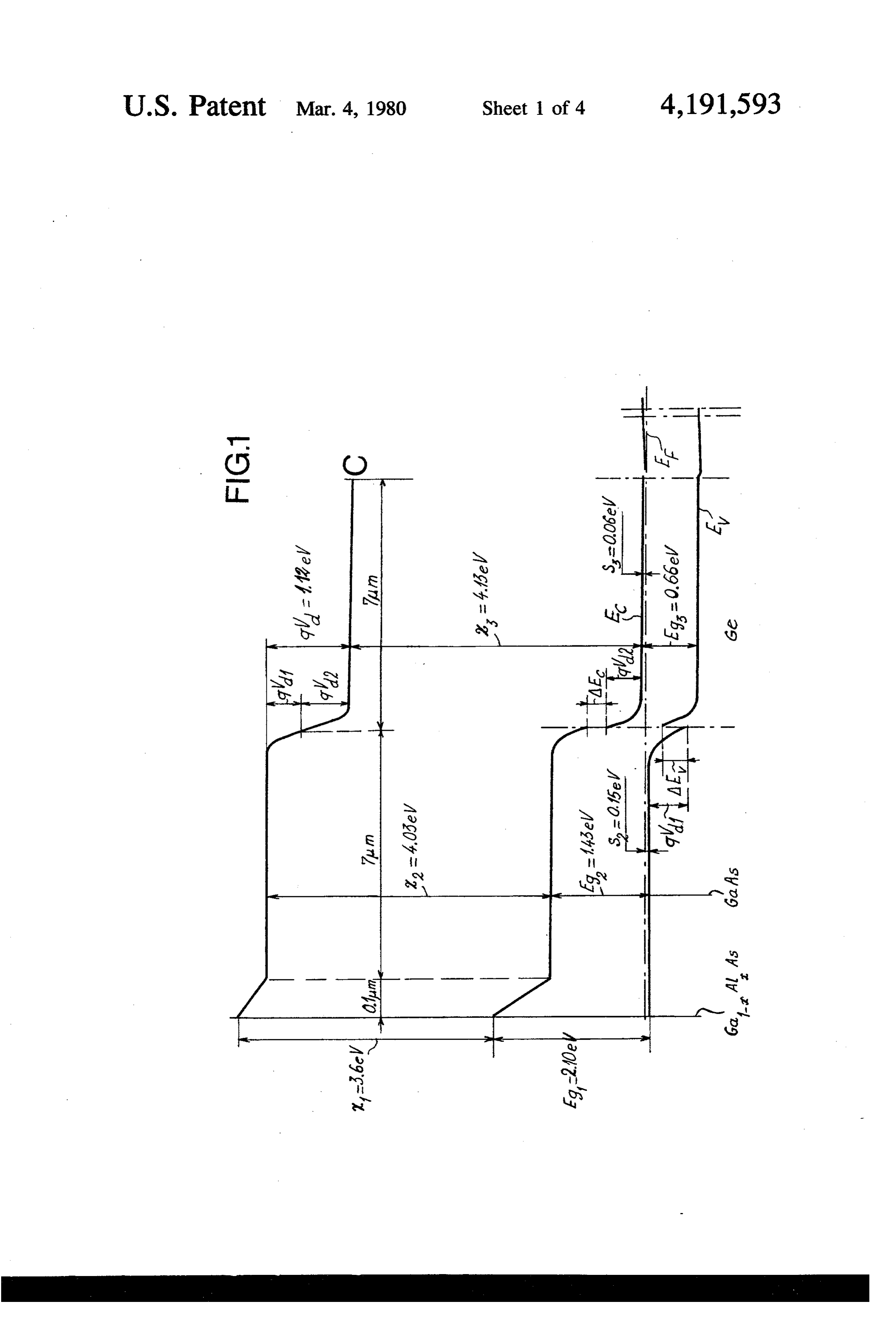
Hovel, Academic Press, 1975, pages 138 and 196. This 30 FIG. 1 is a diagram showing the energy bands and the structure is improved by adding a layer of pCaAs be energy-band discontinuities for the GaAlAs-AlAs and tween the two semiconductor materials to form the Ge-GaAs heterojunctions;
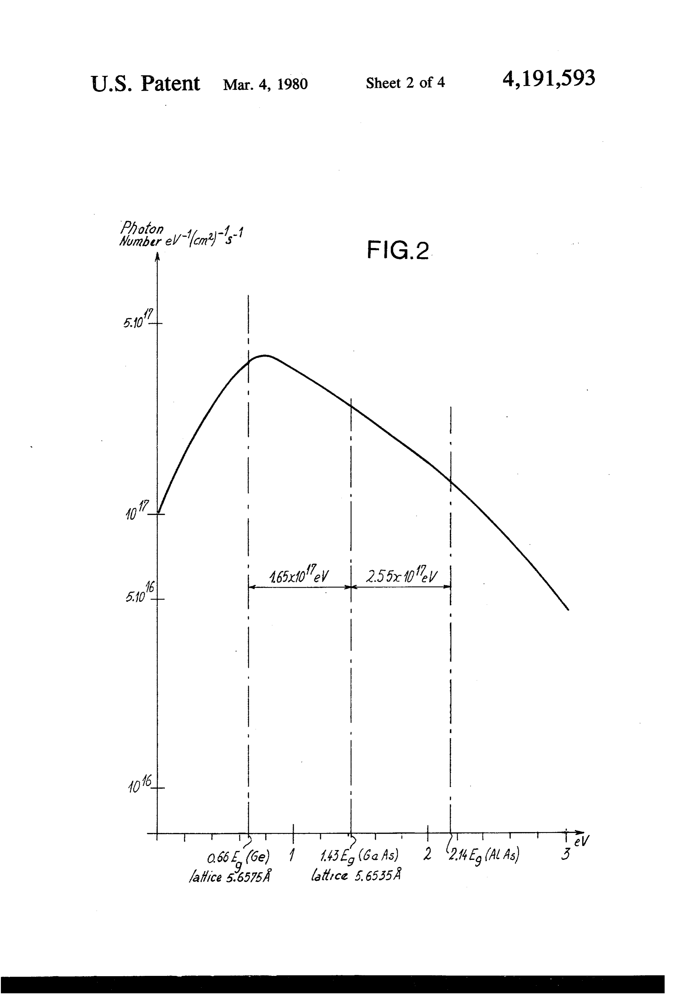
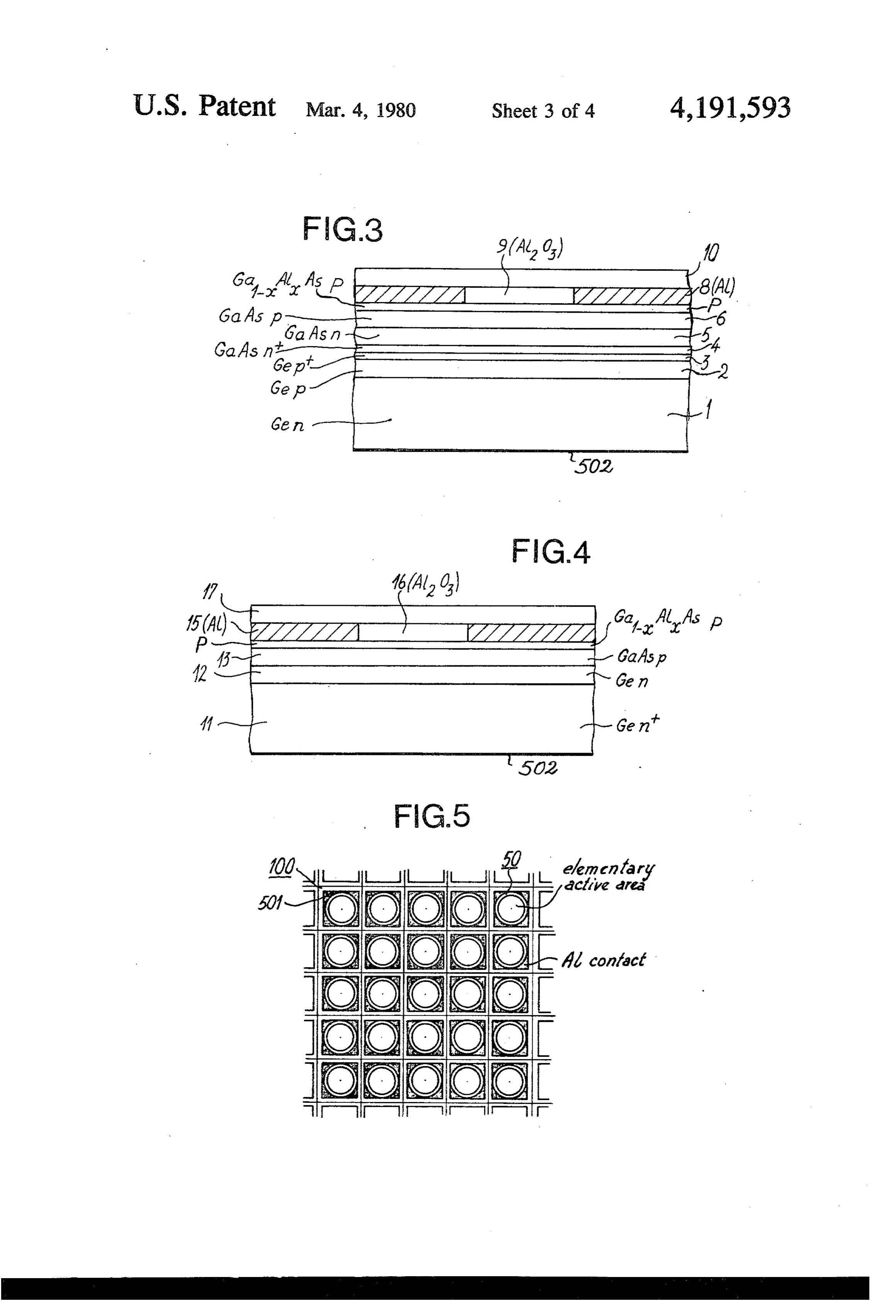
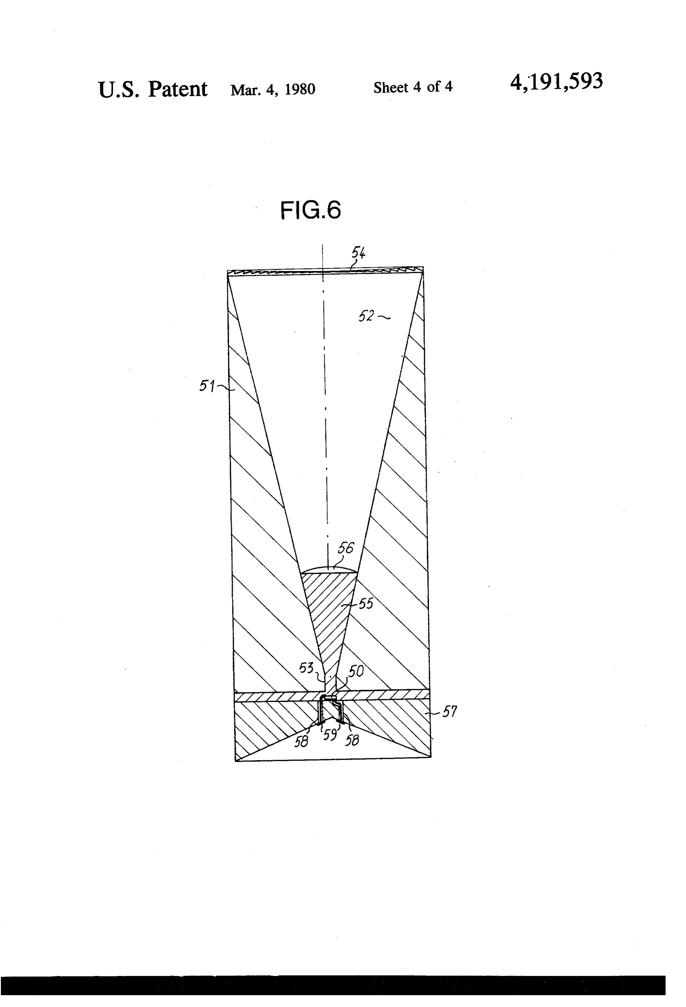
pGa1-xAl-As-pGaAs- nGaAs structure which makes FIG. 2 represents the solar spectrum and the photons it possible to collect carriers over a greater distance absorbed by each of the heterojunctions; compared to the pure heterojunction. FIG. 80 in the 35 FIG.3 represents a first double-heterojunction solar aforementioned publication shows the energy efficiency cell in accordance with the invention; of this structure in AMO (no atmosphere) and in AMI FIG. 4 represents a second double-heterojunction (at the Earth's surface) as a function of the depth of the solar cell in accordance with the invention; and pGaAs layer. FIGS. 5 and 6 represent in diagrammatic form a solar cell device in accordance with the invention.
SUMMARY OF THE INVENTION FIG. 1 shows bands and band energies in terms of the The double heterojunction solar cell of the invention explinations given in the introductory part. It indicates uses as its first heterojunction the heterojunction the values of Egl, Eg2 and Eg3 which are the bandgap energies for GaAlAs, GaAs and Ge respectively, the pGa1-xAll As-noiaas 45 conduction-and valence-band energy discontinuity values AEC and AEw for the heterojunction GaAs-Ge which has just been recalled and the fabrication of GaAlAs, and the electronic affinity values x1, x2 and x3 for which is described on page 195 of the reference publica GaAs and Ge respectively. tion of Hovel. This junction absorbs photons between 50 Referring to FIG. 2, we have shown the solar spec Eg=2.14 eV and E2=1.43 eV. The second hetero trum expressed in number of photons per cm per sec junction is, in compliance with the invention, a Ge ond in a band width of 1 eV in terms of the wavelength GaAs one which absorbs electrons between Eg2=1.43 GaAs, expressed in electron-volts and the bandgap energies for eV and E3=0.66 eV. Eg(GaAs)=1.43 eV and AlAs, Eg(ALAs)=2.14 eV The lattice constants of the heterojunction Ge-GaAs 55 have been marked on the energy axis. The spectrum energy absorbed by the first heterojunction is the area are:
of the spectral curve lying between 1.43 and 2.14 eV; it
In accordance with the invention, the second hetero
Aa = a Ge - a GaAs = 0.004 A junction is an GaAS-Ge one. The bandgap energy of 60 Ge is E(Ge=0.66 eV. The spectrum energy absorbed which give a lattice mismatch Aa/a of 0.07%. by the second heterojunction is then equal to The distance between dislocation is: 1.65x10¹⁷ eV, i.e. a total of 4.20x10¹⁷ eV for the two Ld=a/Aa-0.8 um heterojunctions.
Ge and GaAs have crystallographic lattice dimen
The number of dangling bonds per cm2 is propor 65 sions of 5.6575 and 5.6535 A respectively and conse quently provide, in this respect, a good matching equal tional to the reciprocal of the dislocation distance to 40/56555-7/10000. Their expansion coefficients are squared 1/(0.8x10-)-1.5x108 cm2 5.8x10⁻⁶ and 5.9x10⁻⁶ respectively, i.e., a relative 8 difference of 1.7%. The Ge-GaAs heterojunction can the smaller of the two currents IGe and IGAs which are therefore be made with no difficulty and it withstands both of the order of 25 mA. The output voltage is: high temperatures without dislocation. The epitaxial VGe--VGas-tunes(0.4+1-0.05) volts=1.35 V. deposition of GaAsP and GaAs on Geis disclosed in the article "Epitaxial Deposition of GaAsP on Ge sub The output power per cm is: strates' by H. JAGER and E. SEIPP published in J.
Appl. Phys. 49 (6) June 1978, pages 3217 and 3323. P=1.35X25x10-3-34 mW/cm2.
Description of the preferred
Embodiments 10 example ii
We now describe two examples of double The initial wafer is in n-type Ge with a thickness of heterojunction solar cells with adjacent absorption bands: 400 um having a resistivity of 0.3 to 0.5 ohm-cm and a diffusion length. Lp=10 um. The following layers are
EXAMPLE 1 5 then provided diffusion or epitaxy:
The initial wafer is p-type Ge with a thickness of 400 layer 11 of n-type Ge doped with lithium with a um having a dopant concentration of 6X 1015cm -3 and depth of about 400 um (more precisely, 400 pum less the depth of layer 12), having a resistivity of 10-3 ohm-cm;
a resistivity of 0.5 ohm-cm. The the following layers are then provided by vapor or liquid phase epitaxial tech layer 12 of n-type Ge with a depth of 7 pm which is niques: actually an unmodified part of the initial wafer; layer 1 of n-type Gedoped with lithium with a depth layer 13 of p-type GaAs with a depth of 4 to 7 am, having a dopant concentration of 2x 1019 cm-3 and a of about 400 am (more precisely, 400 pum less the depth diffusion of layer 2), having a dopant concentration of 1018 cm-3 length L=5 pm; and layer 14 of p-type and a resistivity of 10-3 ohm-cm; Ga1-xAlAs doped with zinc with a depth of 500 to layer 2 of p-type Ge with a depth of 7 pm which is 25 2000 A, having a dopant concentration of 2x109 cm3 and a resistivity of 5x10⁻³ ohm-cm for x varying actually an unmodified part of the initial wafer; from 0 to 0.85–0.9.
layer 3 of p-type Ge doped with gallium with a depth of 500 R having a dopant concentration of 100 The cell is coated with a contact 15 of aluminum cm-3 and a resistivity of 6X 10-ohm-cm; having windows 16 of aluminum oxide of a depth of layer 4 of n-type GaAs doped with tin with a depth 30 2500 A.
of 500 A, having a dopant concentration of 109 cm-3 The cell in example II is equivalent to two photodi and a resistivity of 3x10 ohm-cm; odes in parallel. The output current is the sum of the layer 5 of n-type GaAs doped with tin with a depth of two currents Ge and GaAs which are both approxi 5 to 7 um having a dopant concentration of 6X 10⁷ 35 mately 25 mA. The output voltage is the greater of the cm3 and a resistivity of 3.5x10⁻³ ohm-cm; two voltages VGe and VGAs, i.e. i volt. The output layer 6 of p-type GaAs with a depth of 0.3 to 0.5 p.m, power per cm2 is:
having a dopant concentration of 2x 1019 cm-3; and P=(2x25x10-3)x 150 mW/cm2 layer 7 of p-type Ga-Al. As doped with zinc with a depth of 500 to 2000 . having a dopant concentration In the two above examples, the specific dopants for of 2x 1019 cm-3 and a resistivity of 5x10⁻³ ohm-cm. each layer have been described. It goes without saying The composition of this layer varies from x=0 at the junction with pCaAs to x=0.85 to 0.9 at the outer sur that a dopant can be replaced by any other dopant of the same physical properties.
face.
Referring now to FIGS. 5 and 6, we have shown
It should be noted that layers 5, 6 and 7 form a 45 double-heterojunction pGa1-xAl As-pGaAs-nCaAs type solar cell as was multilayer wafer 100 after coat discussed at the outset. These cells are fabricated by ing with contacts 8 and windows 9 but before the appli liquid phase epitaxy (LPE) by bringing a melt consist cation of antireflection layer 10. The wafer is divided up ing of Ga, Al, Zn and GaAs into contact with an n-type into 50 elemental cells and connections with the front GaAs substrate and leaving it to cool for a few degrees contacts 501 and rear contacts 502 (see FIG. 4) put in starting from 900 C. at a cooling rate of 0.1 to 0.5 C. 50 place. In a typical arrangement, as shown in F.G. 5, the per minute. During this reaction, the zinc diffuses into aelementary circle with cell is a 1x1 mm square and the window is a diameter of 0.9 mm and a surface area of the GaAs substrate and forms a p-n junction.
The cell is coated with a contact 8 of aluminum hay 0.63Themm2. cell device in FIG. 6 includes a parallelepipedal ing windows 9 of aluminum oxide of a depth of 2500 A.
The contact and the windows are coated with a poly 55 unit 51, of aluminum for example, with a conical or merantireflecting layer 10 (polycarbonate or methacry pyramidal cavity 52 whose base forms the upper part of late). The indices of layers 7, 9 and 10 are n1 = 1.4, the unit and whose apex is located almost on the lower n2 = 1.7 and n3=3.2 respectively. These layers form an side. Cavity 52 is extended by a cylindrical hole 53 with antireflecting two-layer system between the ambient air a circular or square base which opens out at the lower and the nearest semiconductor to the surface. The mini side and has virtually the same surface area as the cell. mum reflectivity is given, as is known, by: A Fresnel lens 54 is located on the upper side of the unit, above the cavity. The lower section of cavity 52 and hole 53 are filled with the same material 55 as that comprising the antireflecting coating 10, the surface of
This results in a minimum reflectivity of 8%. 65 the said material being shaped into the form of lens 56. The cell in example 1 is equivalent to two photodi The material 55 constitutes a light conduit. odes in series, in opposition with a tunnel diode, formed An elemental cell 50 is bonded to the center of a by the pGe-nigaas junction. The output current is thermal radiator 57 of anodized aluminium of copper 9 and then unit 51 and radiator 57 are assembled for exam thereof, said insert member being terminated at its ple by brazing in such a fashion that cell 50 is directly upper end by a lens shaped part; and underneath hole 53. As an example, the unit has a against said hole a photovoltaic cell comprising a 24x24 mm square cross-section and a surface area of heterojunction between a first layer of Ga1- A 567 mm2. Its height is 49 mm and the distance between 5 As of p-type conductivity and a second layer of lenses 54 and 56 is 40 mm. Insulated connections 58 pass GaAs of n-type conductivity, x varying from 0 at through radiator 57 and terminate in pins 59. the junction of the first and second layers to sub The solar concentration provided by the optical sys stantially 0.9 at the outer face of the first layer; a
I claim: 10 homojunction between a third layer of Ge of p 1. A photovoltaic cell device comprising: type conductivity and a fourth layer of Ge of n a metal parallelepipedal unit; type conductivity; and a tunnel diode formed by a a tapering cavity inside said unit having a base coin heavily doped part of the second layer and a heav ciding with the upper end of the unit and an apex ily doped part of the third layer which are in communicating with the lower end of the unit 15 contact therebetween.
through a hole; 2. A photovoltaic cell device according to claim 2 a Fresnel lens on the base of the cavity; further comprising a thermal bonded to said unit and to a transparent antireflecting insert member within said said cell.
hole and the part of the cavity near the apex s B
Provenance
- Collection
- Patents citing this work
- Pages
- 9
- Method
- pdftotext (the PDF's own text layer) + pdftoppm 300dpi page scans
- Patent office record
- patents.google.com →
- Source
- Google Patents citing-documents table
- Assignee
- Centre National D'etudes Spatiales
- Published
- 1980-03-04
- Transcribed from
- patentimages.storage.googleapis.com →