

patent · US4316791A
Device for chemical dry etching of integrated circuits
23 February 1982
Text
Page 1bibliographic recordscan →
219 - 121 SR
United States Patent (19) 4,316,791 Taillet (45) Feb. 23, 1982 (54) DEVICE FORCHEMICALDRYETCHING OF OTHER PUBLICATIONS
INTEGRATED CIRCUITS
B. N. Chapman et al., "Triode System for Plasma Etch (75) Inventor: Joseph Taillet, Boulogne, France ing", IBM Tech. Disc, Bull, vol. 21, p. 1197, (1978). S. Bhattacharaya, "System for Varying the Directional Assignee: Office Nationale d’Etudes et de ity in Plasma Etching', IBM Tech. Disc, Bull, vol. 20, p. Recherches Aerospatiales, Chatillon, 991, (1977).
France B. N. Chapman, "Plasma Etching of a Positively Biased (21) Appl. No.: 179,788 Wafer', IBM Tech. Disc. Bull, vol. 22, pp. 1175-1176,
22 Filed: Aug. 20, 1980 Primary Examiner-Aaron Weisstuch Attorney, Agent, or Firm-Lowe, King, Price & Becker (30) Foreign Application Priority Data 57 ABSTRACT Aug. 22, 1979 France ................................ 79.21128 Apparatus for dry chemical etching caused by ion bom Int, C. ......................... C23C 15/00; C23F 1/00 bardment of a substrate placed in a vacuum chamber. 52 U.S. Cl. ................................ 204/298; 204/192 E; The substrate is in contact with an electrode, connected 156/345; 156/643 to a high frequency bias voltage source having one 58 Field of Search ........................... 204/192 E, 298; terminal connected to a ground of the chamber. The 156/345, 643 etchants are produced in the form of plasma by an elec trical discharge maintained in the chamber containing a (56) References Cited gas or a suitable gaseous mixture. The plasma is pro duced by a microwave generator and the bias voltage
4,160,690 7/1979 Shibagaki et al. ................., 156/643 amplitudes and frequencies of the two sources enable 4,222,838 9/1980 Bhagat et al. ........ ... 204/192 E the base of a groove on an electronic circuit to be 4,229,233 10/1980 Hansen et al. ....................... 148/1.5 etched without erosion of the groove. 4,233,109 11/1980 Nishizawa ........................... 156/643 4,253,907 3/1981 Parry et al. ......................... 156/643 4 Claims, 2 Drawing Figures
Drawings
Page 2drawing sheetscan →
Page 3scan →
to an ambipolar diffusion of the direct discharge at the
DEVICE FOR CHEMICAL DRY ETCHING OF same electronic temperature. INTEGRATED CIRCUITs - As a result of this alternating potential difference, plasma electrons may be liberated very rapidly if the
Background of the invention
1. Field of the Invention 5 direct potential of this plasma is not sufficiently positive to retain these electrons; it has been shown that the
The present invention relates to the field of the manu direct potential difference, obtained by this effect, and facture of integrated circuits and more particularly to similar to the behavior of a rectifier, is at least equal to the technique of dry chemical etching of the circuits. 10 VV2.
Several types of etching methods enable fine pattern In addition, the thickness of the sheath is linked on ing of integrated circuits to be obtained. The most wide one hand to this direct potential difference, to the elec spread are electron beam etching methods and photo tron density of the plasma and to its electronic tempera etching techniques using dry chemical etching. ture, by Child-Langmuir's law; the sheath thickness is, 2. Description of the Prior Art on the other hand, linked to VA by an equation which Dry chemical etching methods utilize a reagent ele 15 expresses the high frequency potential difference across ment source produced in the form of plasma generated the sheath as the product of the sheath impedance by a high frequency electrical discharge maintained in a through the high frequency current. From these two vacuum chamber containing a gas or a suitable combi equations it is possible to calculate the expression which nation of gases under a low pressure. The discharge gives the potential energy of the plasma ions, i.e. the provides a plasma producing radicals, ions and elec 20 energy which the ions bombarding the substrate would trons which may, with a substrate, provide chemical have if they succeeded in passing through the sheath reactions leading to etching. without colliding with the neutral particles. Apparatuses which enable this dry chemical etching In these circumstances, the energy W of the ions method to be applied comprise a vacuum chamber with 25 bombarding the substrate is given by the equation: an internal electrode supporting the substrate to be etched, which electrode is maintained at the potential of kTX W = 1.26 (op/o)? W- (1) a high frequency power source. The chamber includes metal surfaces constituting a second electrode that is in which:
grounded to the high frequency source. k is Boltzmann's constant, When the HF source is in operation, the gas con 30 T is the electronic temperature of the discharge; tained in the chamber is ionised and becomes a plasma. c)/27t is the discharge frequency; An ion bombardment of the substrate takes place as a op/2t is the frequency of the plasma linked to the elec result of the existence of a direct electrical potential of tron density ne of the plasma by the equation the plasma, this potential being sufficiently positive with respect to the substrate. 35
The above-described prior art is disclosed in an arti o) = nee cle of Yasuhiro HORIIKE and Masahiro SHIBAGAKI entitled "A New Chemical Dry Etching” published in
Proceedings of the 7th Conference on Solid State De in which e is the electron charge, m the mass of the vices, Tokyo, 1975, Supplement to Japanese Journal of 40 electron and eo the dielectric permittivity of vacuum; Applied Physics, Vol. 15 No. 7, 1975, pages 13-18. The W- is the energy with which the high frequency Horiike etal article discloses a method for the selective source provides the average electron of the discharge etching of a material by reagent ions. between two collisions with neutral particles. Recent experiments show that etching is linked to the Equation (1) may also be expressed as follows: ion bombardment of a groove base by energetic parti 45 cles of some hundreds of electron volts, as shown by M. W=(1.262e-2e2m-1 (kT)-20-4A2 (P/s)2 (2) F. WINTERS in the Journal of Applied Physics 49 in which:
The inventor's work in the field of electrical dis A is the mean free path of the electrons of the discharge charges has enabled him to demonstrate that if these 50 and (P/v) is the high frequency power density, P is discharges are applied to chemical etching, it is possible, the power and v is the volume. In order for these in certain conditions, to strike the discharge to etch equations to be applicable, it is further necessary for with an anisotropic nature, i.e. a base of the groove is the thickness of the sheath po of the discharge to be etched much more rapidly that walls of the groove. A lower than the mean free path Ni of the ions of the paper relating to the general properties of the plasma 55 discharge, i.e.
potential in a high frequency capacitive discharge has been published by the applicant in a report of the pos^i, pas W4 (3) Academie des Sciences of Paris Volume 287 dated Dec. In effect one has:
In a high frequency (HF) capacitive discharge, the 60 A=N/4 (4) plasma is maintained by passing an alternating current from a HF generator across sheaths which adjoin elec whence trodes of the HF generator. This current imposes an alternating potential difference on the sheath. If the p-n-(W)/(kt)-loo- (5) frequency of the current is sufficiently low and the 65 power absorbed sufficiently high, the effective value which may also be expressed: VA of this alternating potential difference is much greater than the direct potential difference, VP, coupled p=e-e2m-ioP/s)3/2n-2(kT)-7/43/2 o-3 (6)
Page 4scan →
the chamber comprises a communication aperture with and therefore: a plasma Source.
In a first embodiment of the invention, the plasma 4 e-le2 m (P/)3/2n. (kT).7/Ao-3 s 1 (7) source is a microwave plasma generator. In a further embodiment of the invention, the plasma source is a
If the electrical discharge is maintained at the high hollow cathode source.
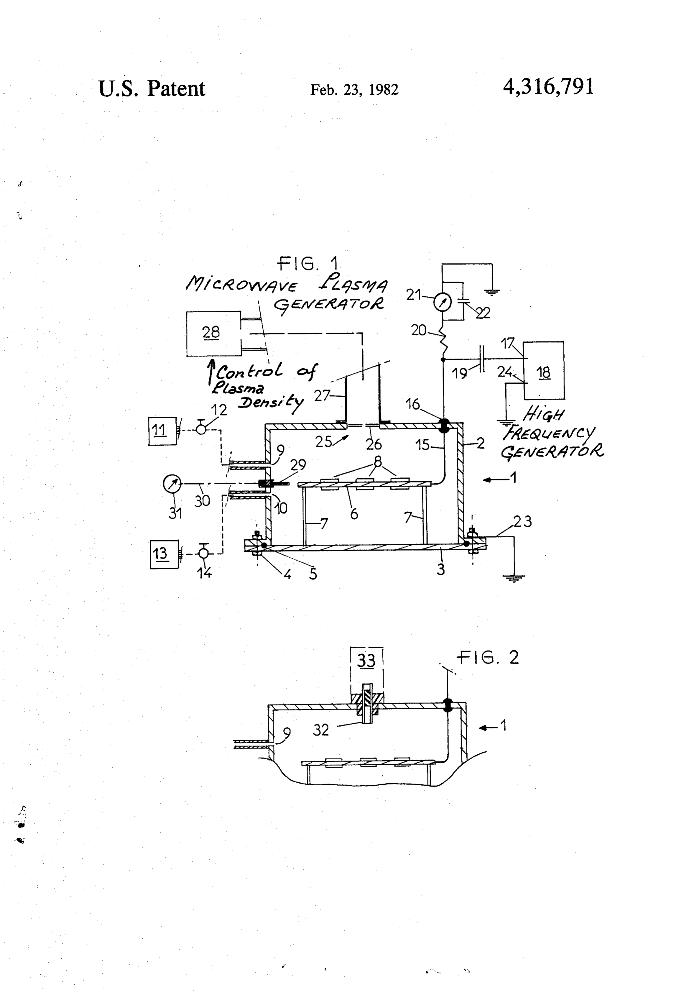
frequency (a)/2)7t, this latter condition is often incom patible with the equations which give the particulate BRIEF DESCRIPTION OF THE DRAWINGS energy amounts of the discharge and which are com The invention will be described in detail with refer plex equations depending on the specific properties of 10 ence to the attached drawings, in which: the gaseous mixtures used. FIG. 1 is a diagrammatic illustration of one embodi 2 In effect, examination of Equations (2) and (7) sug ment of the invention for etching integrated circuits; gests that an excessively high value should not be se and lected for co, to obtain an ion bombardment of sufficient FIG. 2 is a partial view of a further embodiment of energy (for example 100 eV) on the substrate. Condition 15 the apparatus of the invention. (7) can only be obeyed in these circumstances if the DESCRIPTION OF THE PREFERRED value of the electronic density ne is suitably high and if the power density (P/v) is not too high. Simultaneously EMBODIMENTS obtaining the required values is not in general feasible The apparatus comprises a metal vacuum chamber 1 due to the energy balance equations mentioned above. 20 which may be a tuned cavity or a simple tank, com The following examples are cases in which the two posed of belljar 2 having a circular cross-section that is conditions are not achieved simultaneously: connected to base 3 by bolts 4, with the interposition of EXAMPLE 1. a leak-tight joint 5 between the bell jar and bolts. Disposed in the interior of vacuum chamber is a metal 25 electrode 6, electrically insulated from the exterior of o/2n = 13.56 MHz; P-200 Watts; v =5x10⁻³m3; the chamber by dielectric supports 7 fixed to the base 3. kT=8 eV; X =3X 10⁻³ m; ne=4x10¹⁶ m3; The electrode 6 is shaped as a thick disc on which the W- = 1.25 x 10⁻² eV; (op/o)= 1.75x10; substrates 8 to be etched are fastened. Belljar 2 includes V=9500 v and pe= 1.5x10⁻²m parts 9 and 10 which respectively communicate with 30 ducts connected to a pumping system 11 and a gas intro
The condition A24po is not obeyed.
Example 2
duction system 13; systems 11 and 13 are respectively connected to ports 9 and 10 via adjustable valves 12 and if 14.
The electrode 6 is electrically connected to one ter kT=8 eV; A=3X 10⁻³m; ne=4x10¹⁶ m-3; minal of lead 15 that extends through bell jar 2 via an W- = 1.25x10⁻³ eV; (o/o)= 1.75x 10⁻⁴, insulated, leak-tight grommet 16. A second terminal of V=59 V and pe=0.5x10⁻³ m lead 15 is connected by way of a capacitor 19 to a termi The condition W24po is achieved but it is not possible nal 17 of a high frequency power source 18, having a to obtain an electronic density of 4x10¹⁶ m-3 with a frequency between 1 and 30 MHz, for example the power of 20W in 5X 10⁻³ m; this case may not there standard frequency of 13.56MHz. The second terminal fore be achieved in practice. of lead 15 is connected to ground via a series circuit including resistance 20 of high value, for example
SUMMARY OF THE INVENTION greater than 10 MS) and ammeter 21 shunted by a ca The object of the invention is to provide a suitable 45 pacitor 22.
means of dispensing with the restrictions linked to the The bell jar 2 forms a second, grounded electrode energy balance equations dependent on the specific having a ground connection 23; terminal 24 of the high properties of the gaseous mixtures used. The restrictions frequency source 18 also being connected to ground. are eliminated so it is possible to simultaneously obtain ingThe vacuum chamber 1 includes means for establish a sufficiently low value for the high frequency power 50 the aceiling fluid flow with a plasma source. For this purpose, of chamber 1 has an aperture 25 provided density (P/v) and a sufficiently high value for the elec with tron density ne so it is possible to satisfy condition (7). to a microwave iris a coupling 26 and a wave guide 27 connected
In the method of the invention, integrated circuits are can be adjusted between 3 28, generator and having a frequency that etched by exposing a substrate to be etched to a plasma On the internal wall of chamber 1 is a Langmuir produced in a leak-tight chamber containing a gas or a 55 probe 29, connected by lead 30 to a device for display gaseous mixture under a low pressure. The substrate is ing the plasma density 31.
disposed on an internal electrode biased by a high fre quency voltage. The plasma is produced by a plasma theByEquations means of the use of the above arrangement, only (3) and (4) must be considered with the source which is independent of the bias voltage source. following Equations (8) and (10). The operation can be An apparatus for applying the method of the inven 60 described from the known equation: tion comprises a leak-tight metallic chamber containing a gas or a gaseous mixture under a low pressure. An p=5/she-ne-2(kT) - V. (8) internal electrode insulated from the chamber supports the substrate to be etched. A second electrode that If it is assumed that the starting data are: connects of the internal electrode to the wall of the 65 1/ The pressure p under which it is intended to carry chamber is biased by a high frequency voltage source. out the etching,
A gas or a suitable gaseous mixture is introduced into 2/ The acceleration voltage V considered optimum to the chamber as well as evacuation means. The wall of obtain the desired rate of anisotropy.
Page 5scan →
The selection of a pressure p provides T without The use of a high frequency alternating voltage for ambiguity. By considering Equation (3), posN/4, and the biasing of the electrode 6 enables the insulating replacing the physical constants of Equation 3 known substrates to be biased with respect to the plasma. values thereof, Equation (8) becomes the inequality: The following is a summary of the adjustment method for the apparatus in order to carry out the method of the invention:
ne 2 1.4 x 10⁸A { E- Vp the acceleration voltage V is selected;
the microwave generator 28 is adjusted to obtain a satisfactory density defined by Inequality (9);
in which kT is the electron temperature measured in 10 Vis adjusted by calculating it from the Formula (10) electron volts. For example, if the mean free path is one where IA is the value of the direct current read on am millimeter (10-3m) and kT =6 eV, n.25.7x1016m-3. meter 21.
The microwave generator 28 is adjusted to produce In FIG. 2, the ceiling of the bell 2 of the vacuum the minimum electron density defined by the above 15 municates1 front chamber is provided with an aperture with that com portion 32 of a hollow cathode plasma inequality (9).
The selected acceleration voltage V is obtained by trigger system. generator comprising a supply and generator 33, this adjusting the high frequency source 18,
In the microwave discharge the sheaths are of negli hollow The apparatus is adjusted as in the case of FIG. 1, the cathode having been previously triggered.
gible thickness and the plasma potential is very close to 20 The anisotropic ground. By connecting the electrode 6 that carries the an increase in the density etching obtained as indicated enables substrate 8 to be etched to the HF voltage source 18, an be etched and enables the of the etches on a substrate to invention to be applied to the additional sheath of considerable thickness is formed manufacture of large scale integration (LSI) circuits. about the electrode and a direct voltage V of suitable I claim:
polarity appears between the electrode and the plasma. 25 1. An apparatus for etching integrated circuits com This encourages ion bombardment. prising:
The following equation links voltage V to the in a generator of a plasma of a gaseous component jected alternating current density I/S (S being the total under low pressure;
surface area of the electrode in contact with the means for controlling the electron density of the plasma): 30 plasma formed by said plasma generator; a leak tight chamber having a metallic wall and an
V-1.58,e-2e-in-2 o-' (kT)-1 (I/S) (10) inner metallic electrode plate for supporting inte grated circuits to be etched, said plate being insu
It is not, however, necessary for an operator to mea lated from said wall;
sure the alternating current I in order to adjust the 35 a high frequency alternating signal generator; apparatus. The voltage V, in effect, appears between means for applying said high frequency alternating the electrode and ground; it is therefore sufficient to signal between said electrode and said wall; read the direct current IA passing through the resistance means for measuring the value of the current of said alternating signal; and 20 and the ammeter 21 in order to ascertain V from the 40 communication -equation: means between the plasma generator and the leak tight chamber.
V=IAR (11) 2. An apparatus as claimed in claim 1, wherein the communication means comprises a waveguide between the plasma generator and the leak tight chamber and a
As the microwave generator 28 has been adjusted as 45 coupling indicated above, the condition (3) is obeyed. As long as iris in said waveguide.
V is less than or equal to a selected value, the ions communication meansapparatus as claimed in claim 1, wherein the accelerated towards the substrate are not subjected to the interior of the chamber enables the emergence within collisions in the sheath. If Vexceeds the selected value, hollow cathode plasma generator. of the front portion of a these collisions take place and the etching becomes 50 4. An apparatus as claimed in claim 1, wherein the isotropic.
Lastly, if V is too low, the ion bombardment effect electrode plate comprises means for connection to becomes negligible and the etching becomes isotropic. high value andconnection ground, said means being a resistance of a an apparatus for measuring direct cur
It is therefore suitable to set V as close as possible to rent intensity.
the selected value. 55 sk k sk. k. k.
Provenance
- Collection
- Patents citing this work
- Pages
- 5
- Method
- pdftotext (the PDF's own text layer) + pdftoppm 300dpi page scans
- Patent office record
- patents.google.com →
- Source
- Google Patents citing-documents table
- Assignee
- Office Nationale D'etudes Et De Recherches Aerospatiales
- Published
- 1982-02-23
- Transcribed from
- patentimages.storage.googleapis.com →