

patent · US4349409A
Method and apparatus for plasma etching
14 September 1982
Text
Page 1bibliographic recordscan →
United States
Shibayama et al.
Patent (19) (11)(45) 4,349,409
. (54) METHOD AND APPARATUS FOR PLASMA FOREIGN PATENT DOCUMENTS
ETCHING
(75) Inventors: Hikou Shibayama; Tetsuya Ogawa, Patent Abstracts of Japan, Vol. 4, No. 71, May 24, both of Machida; Makoto Kosugi, 1980, P., 10E 12, Dry Etching Device, Appl. No. Yokohama; Tokushige Hisatsugu, 53-111257, Fu, Itsu K. K. Kouichi Kobayashi. Chofu; Koichi Kobayashi, Journal of the Electrochemical Society, Vol. 126, Yokohama, all of Japan No. 6, June 1979, Pages 1024-1028, The Roles of Ions and Neutrak Active Species in Microwark Plasma Assignee: Fujitsu Limited, Kawasaki, Japan etching, Suzuki et al.
Ion beam etching, Harper et al, Abstract No. 284.
(21). Appl. No.: 262,793 Journal of the Electrochemical Society, Vol. 80-1, May 1980, Pages 716-717, how Energy Ion beam 22 Filed: May 11, 1981 etching, Harper et al.
(30) Foreign Application Priority Data Primary Examiner-William A. Powell Attorney, Agent, or Firm-Staas & Halsey
May 12, 1980 JP Japan .................................. 55-62427
May 13, 1980 (JP) Japan .................................. 55-62992 57 ABSTRACT - A method and an apparatus for plasma etching semicon Int. Cl........................ H01L 21/302; B44C 1/22; ductor materials by providing an intermediate electrode CO3C 15/00; CO3C 25/06 between the electrodes in a parallel state type plasma (52) U.S. C. .................................... 156/643; 156/345; etching apparatus, moving the intermediate electrode 156/646; 156/653; 204/192 E; 204/298 by a drive mechanism, and continuously changing from Field of Search ................ 156/643, 646, 650-653, a condition of high input power and high self-bias volt 156/345, 657; 204/164, 192 E, 298; 250/531; age to a condition of low input power and low self-bias. 252/79.1 voltage while varying the distance between the inter 56 References Cited mediate electrode and the first electrode and the RF power, thereby to remove damage or deposits that may
4,174,251 11/1979 Paschke .......................... 156/646X tor material was being subjected to processing. 4,233,109 11/1980 Nishizawa ....................... 156/646X 18 Claims, 32 Drawing Figures
MVVVVVV
Drawings
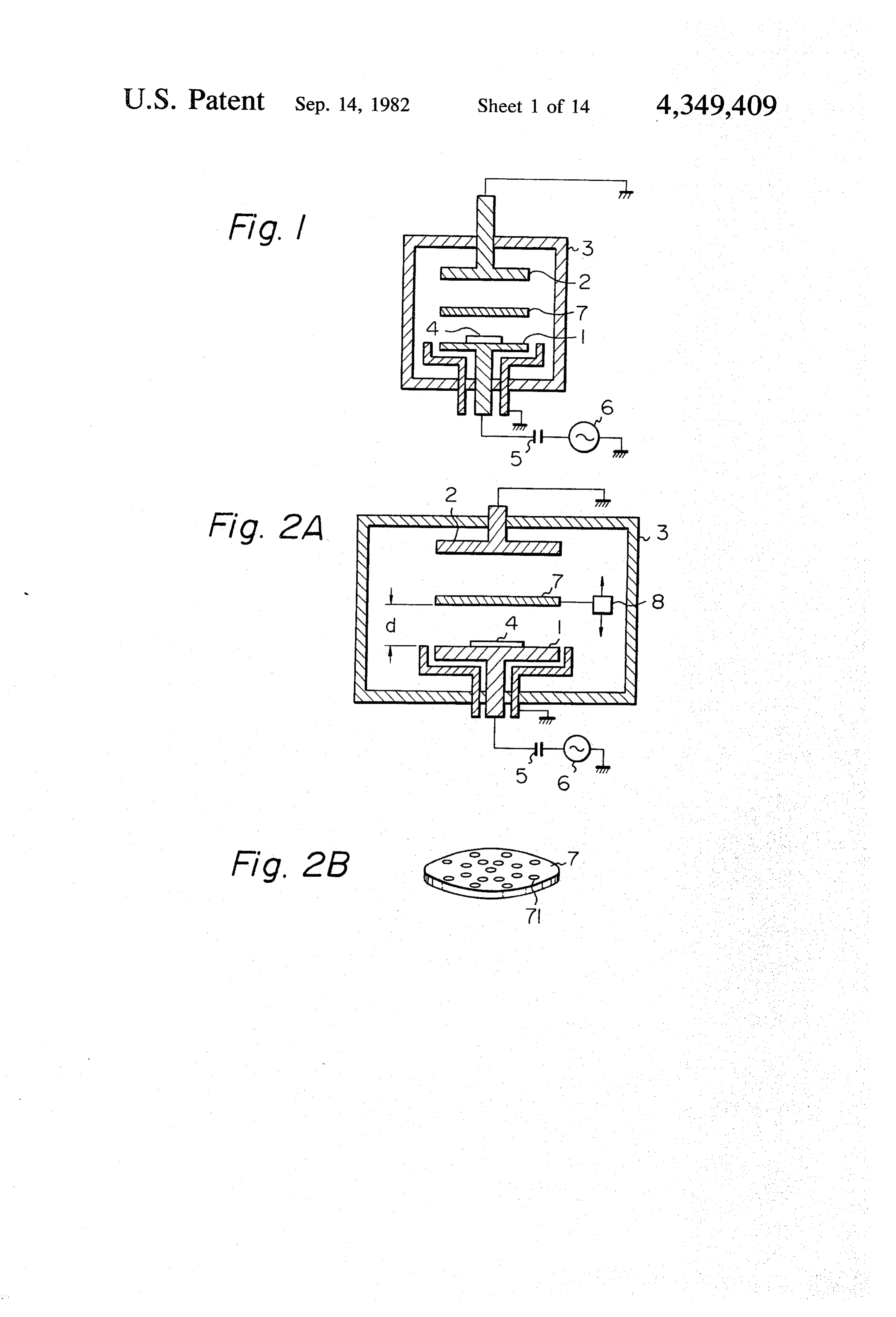
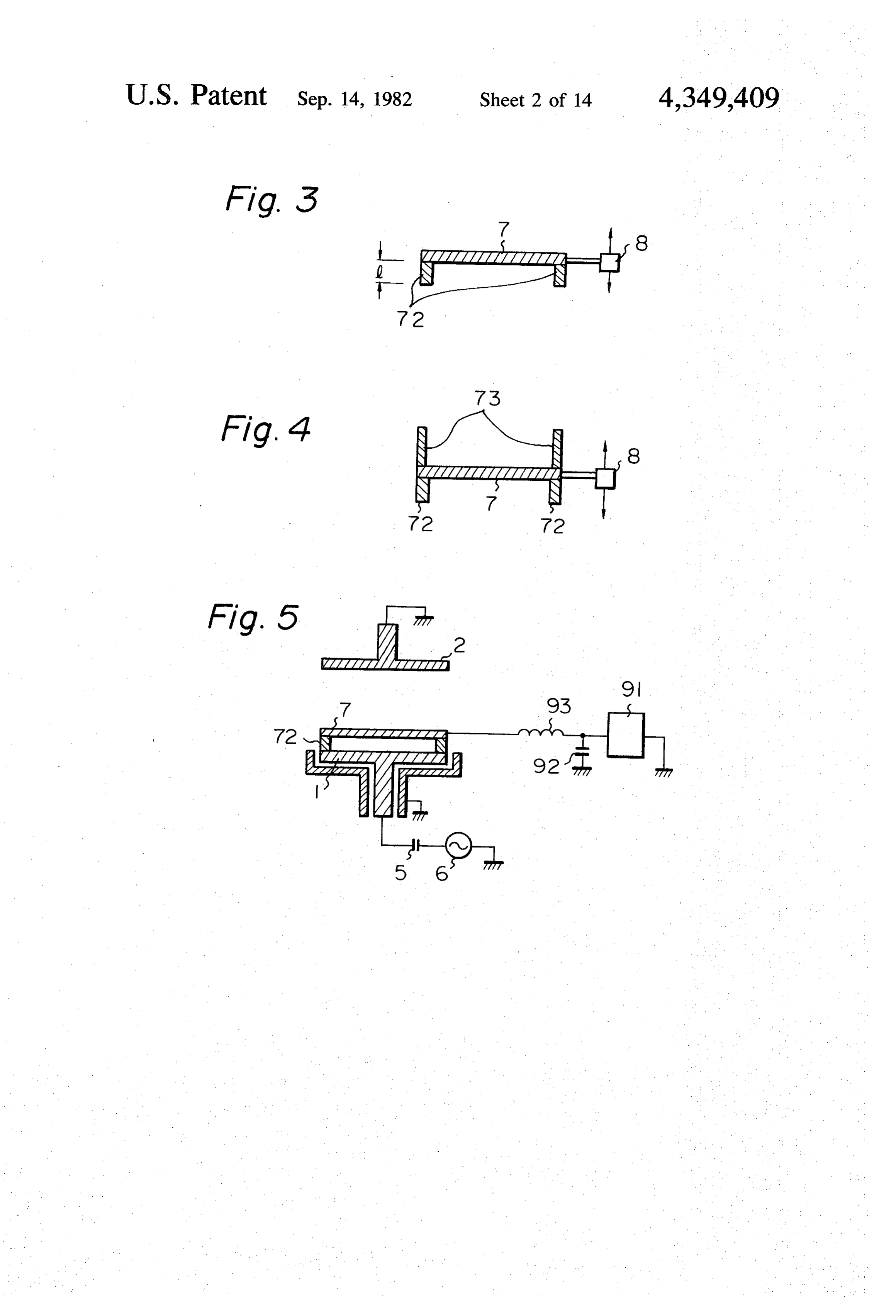
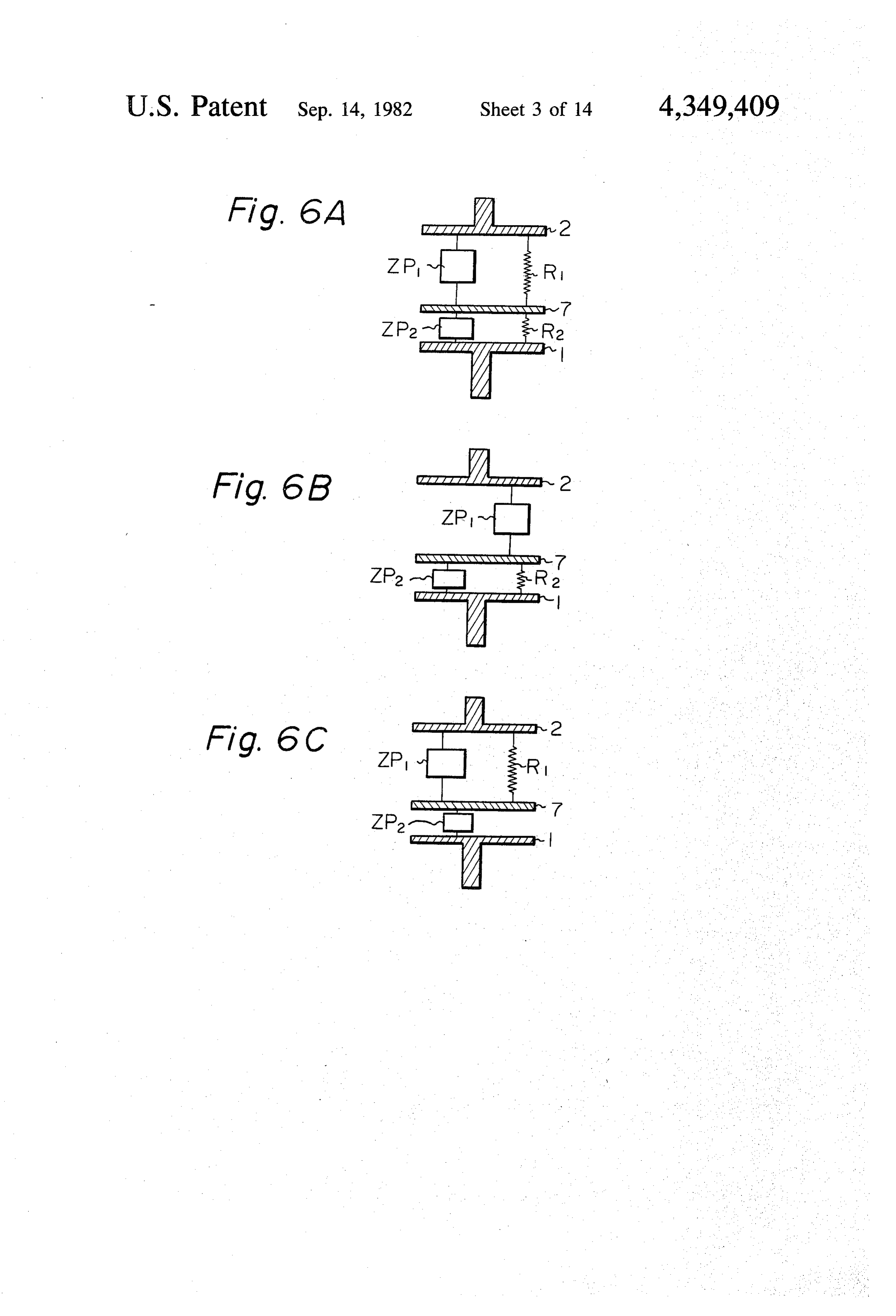
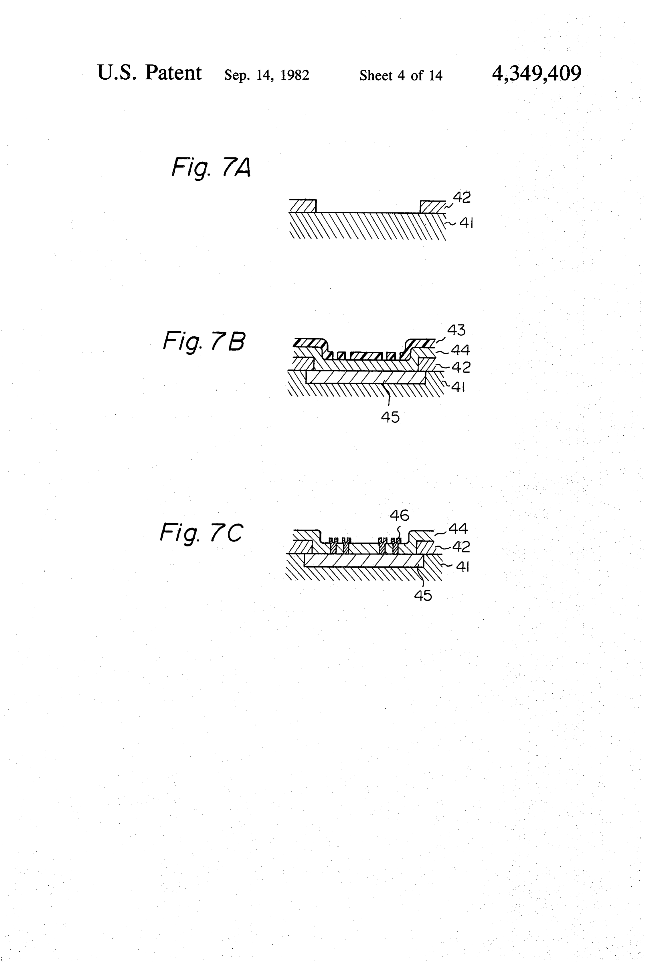
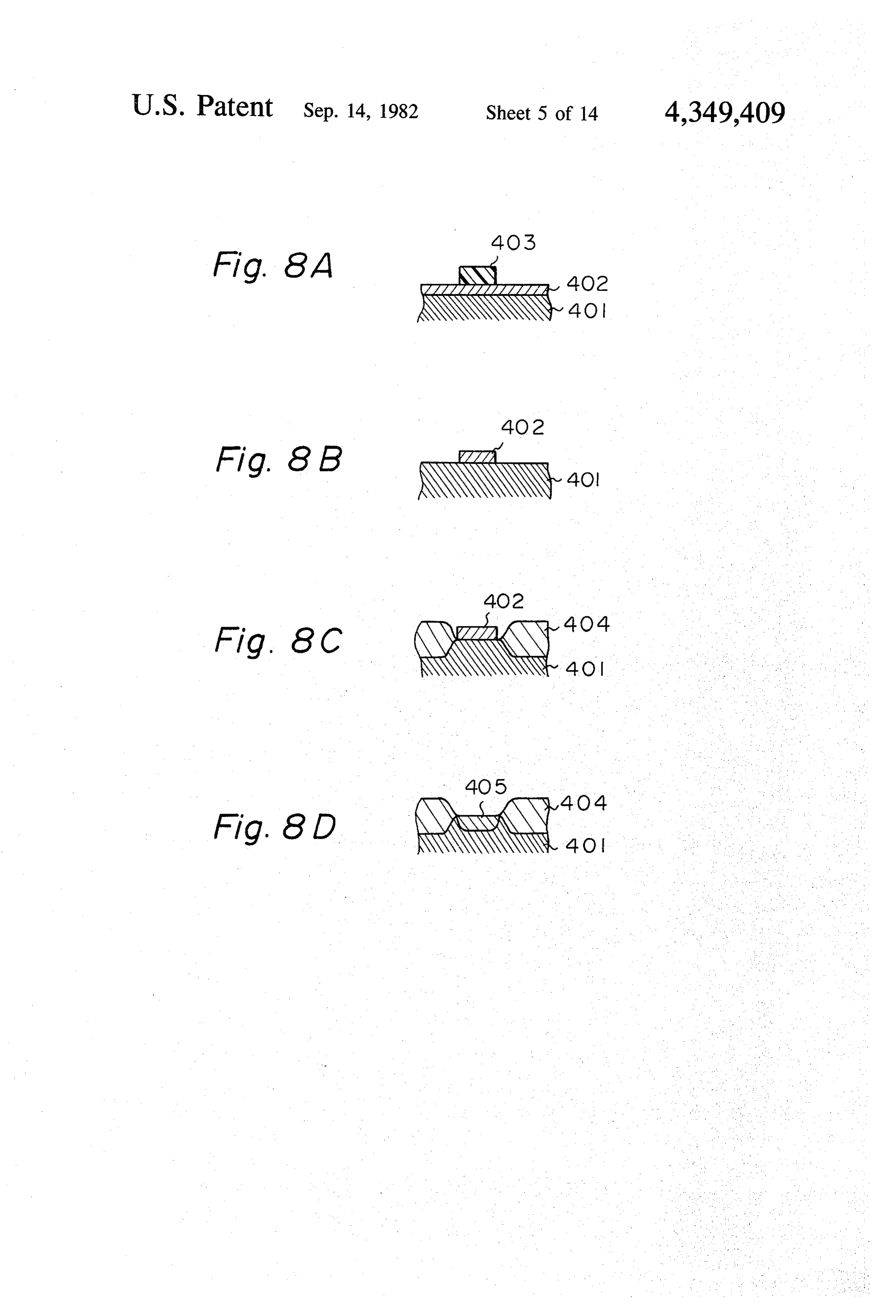
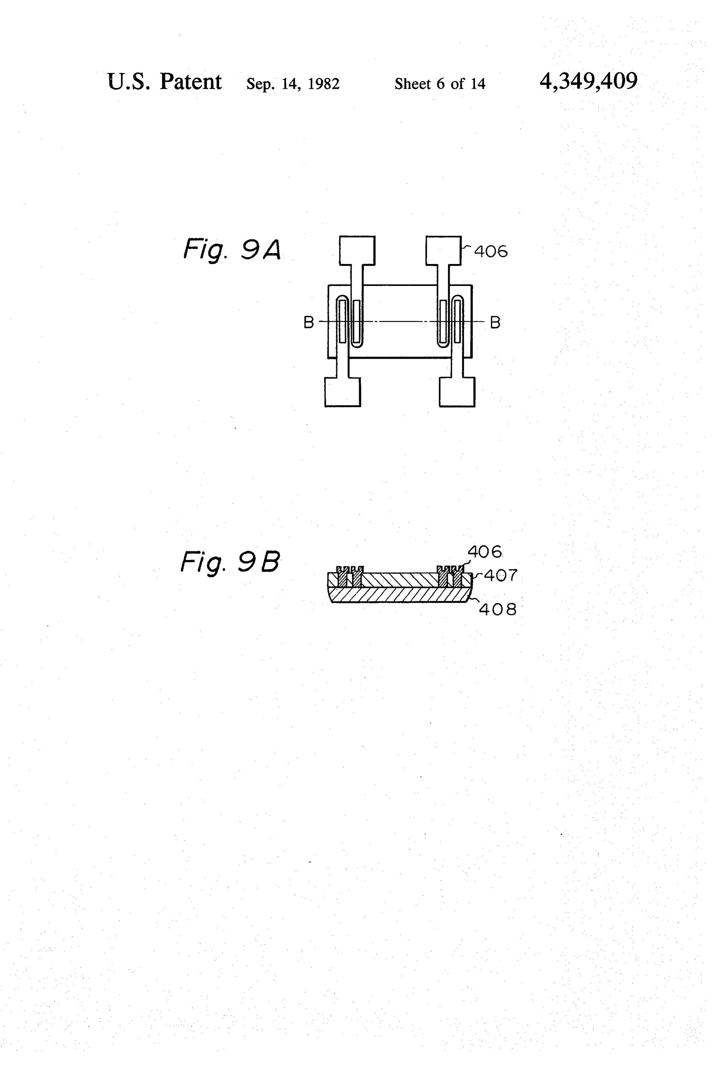
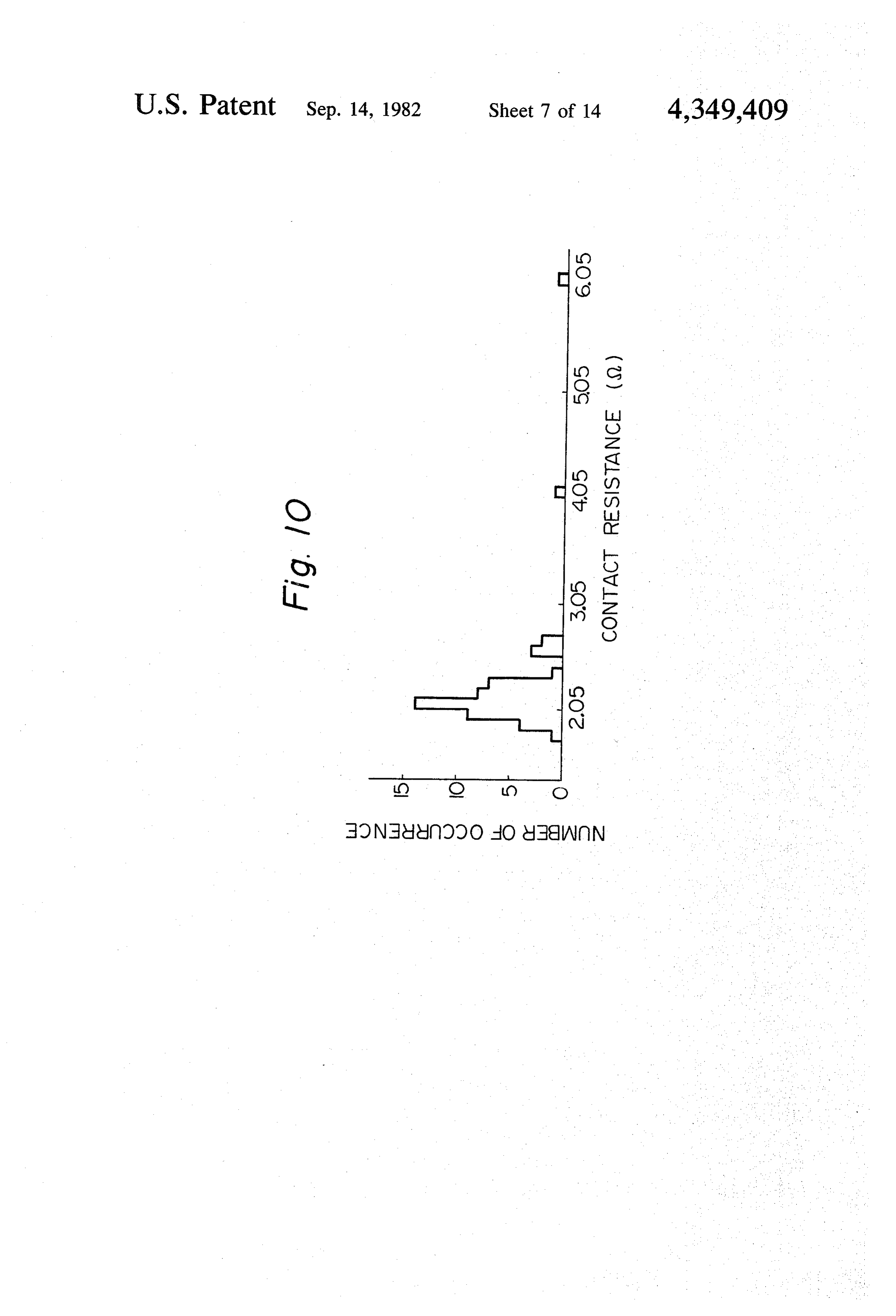
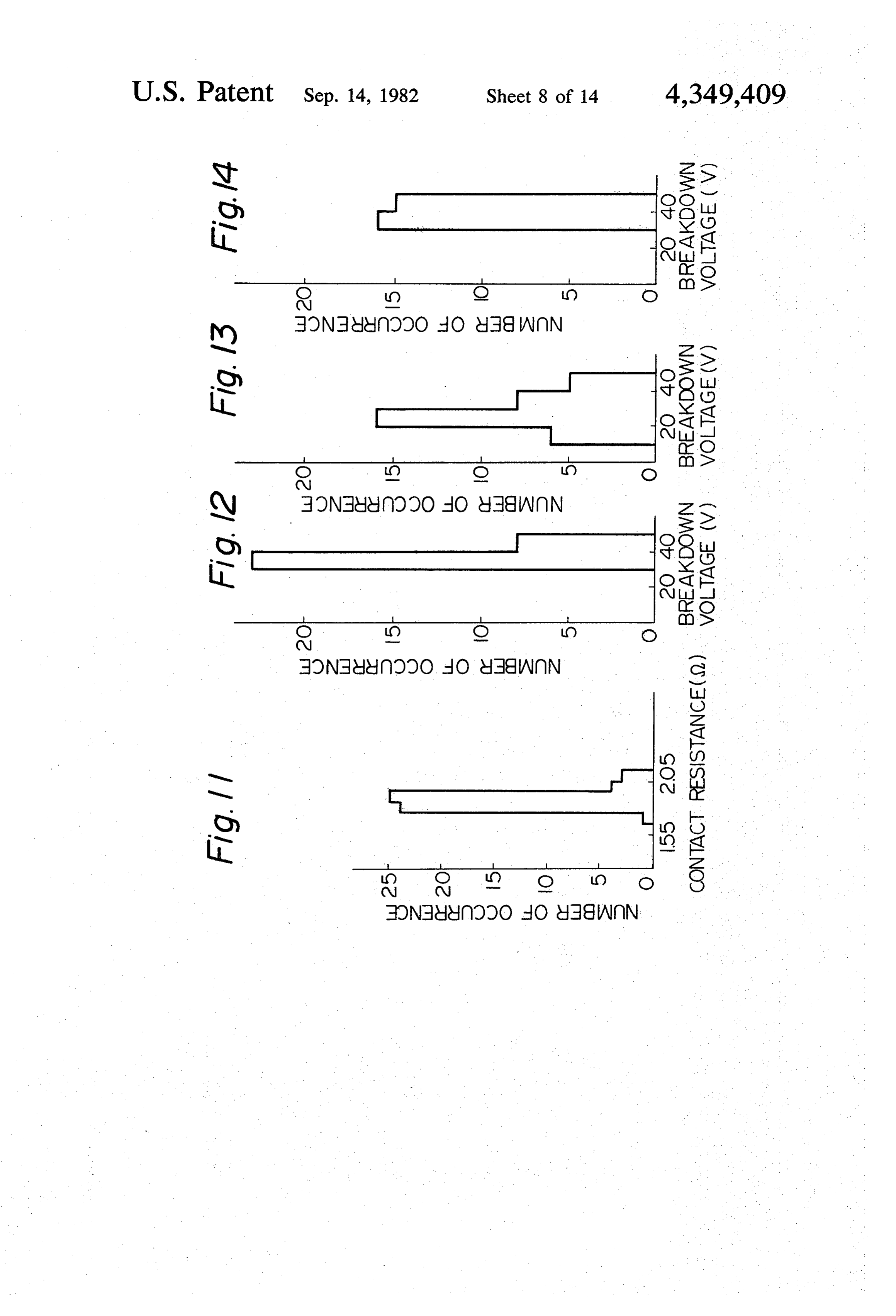
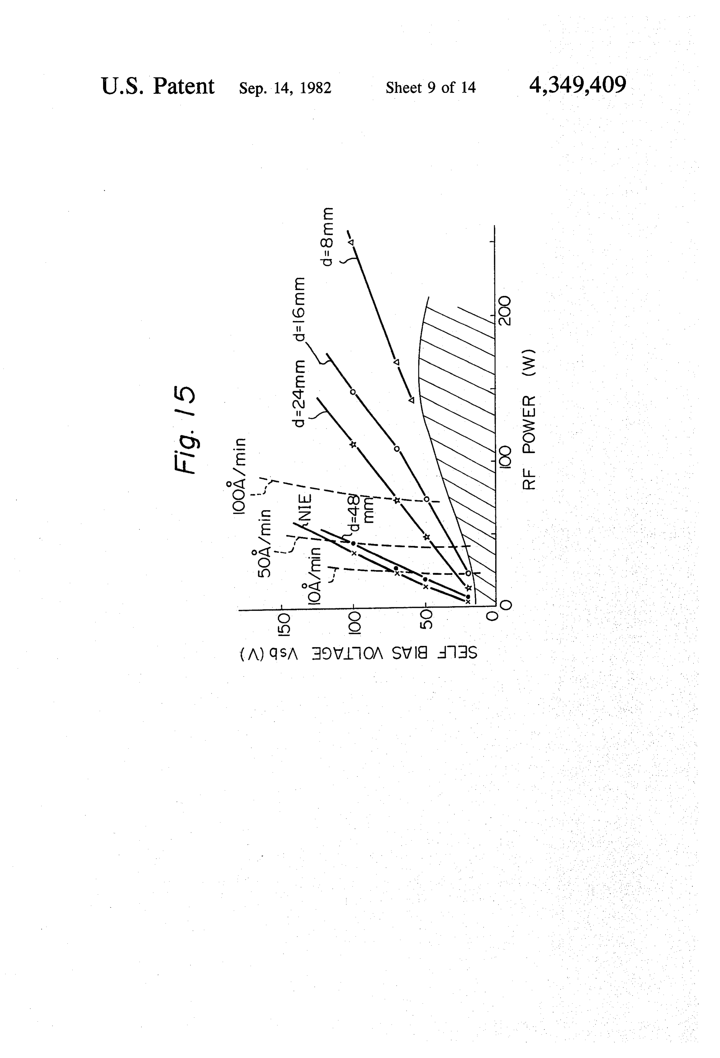
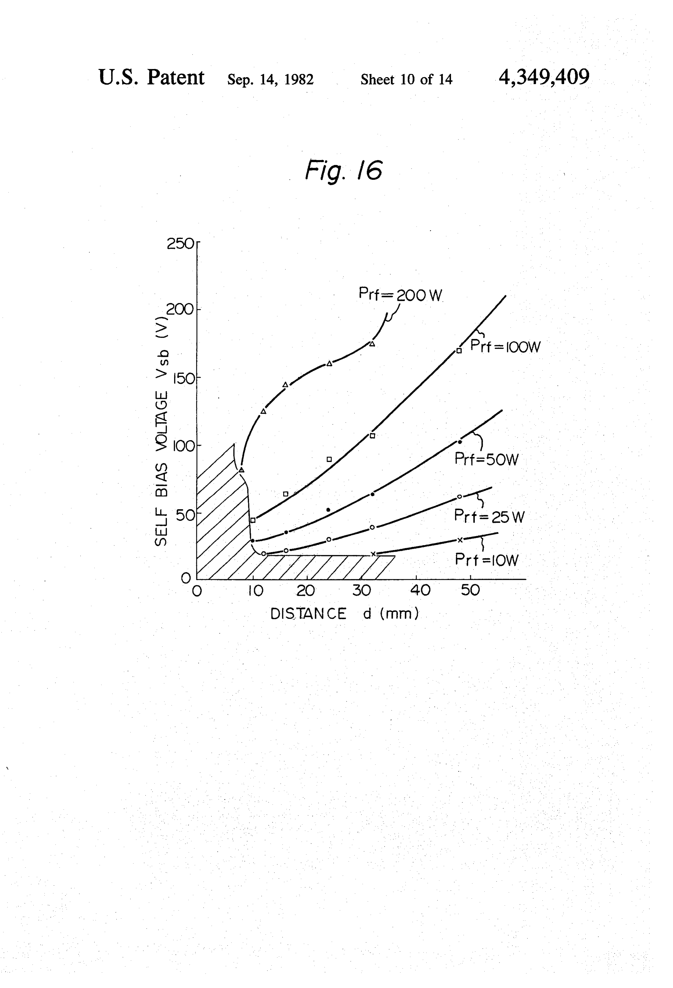
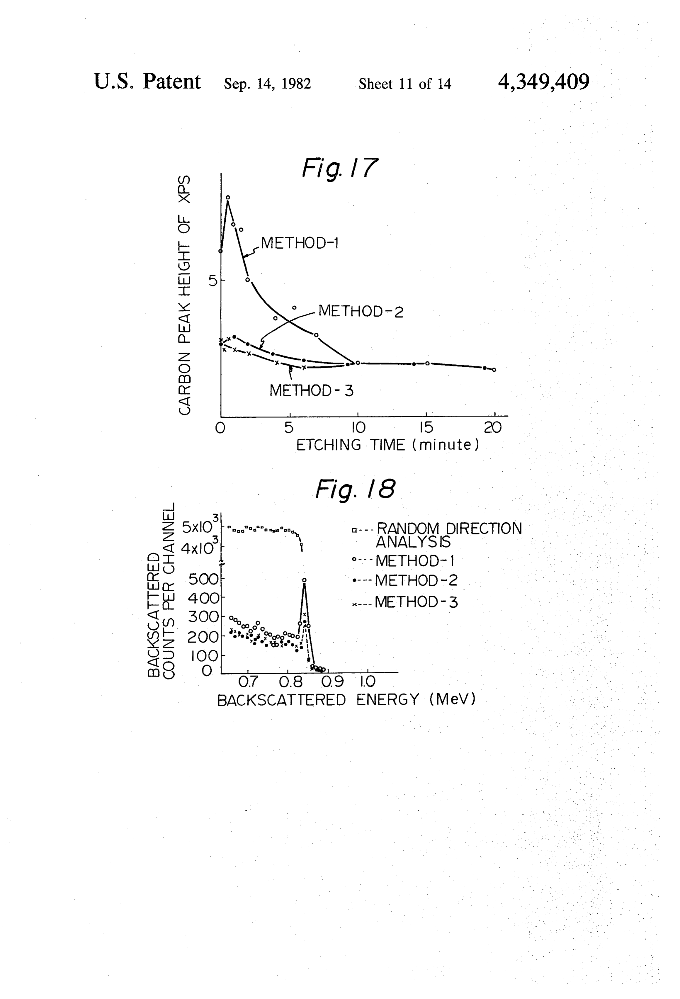
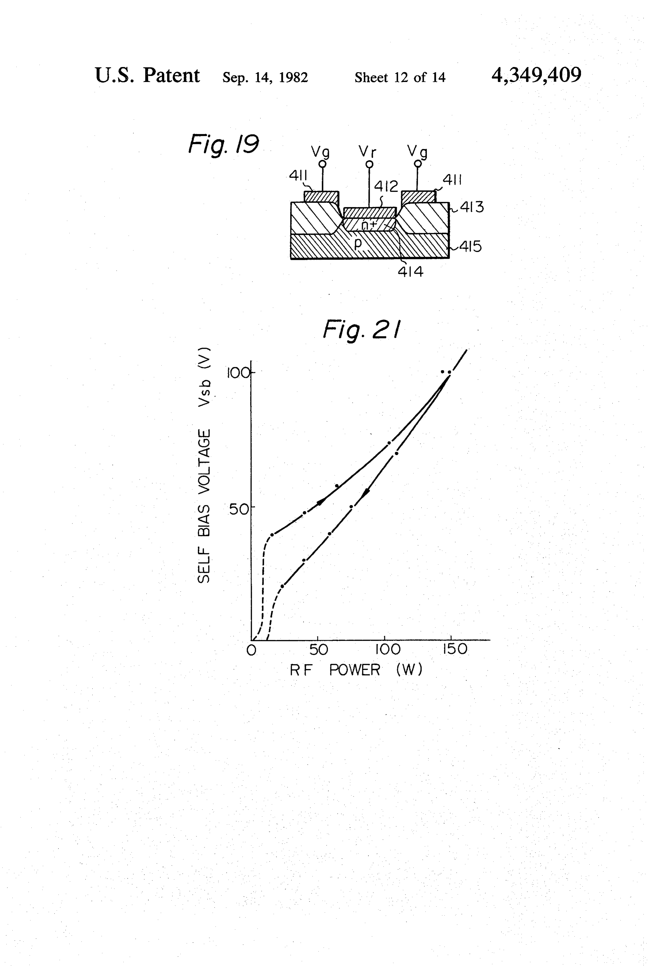
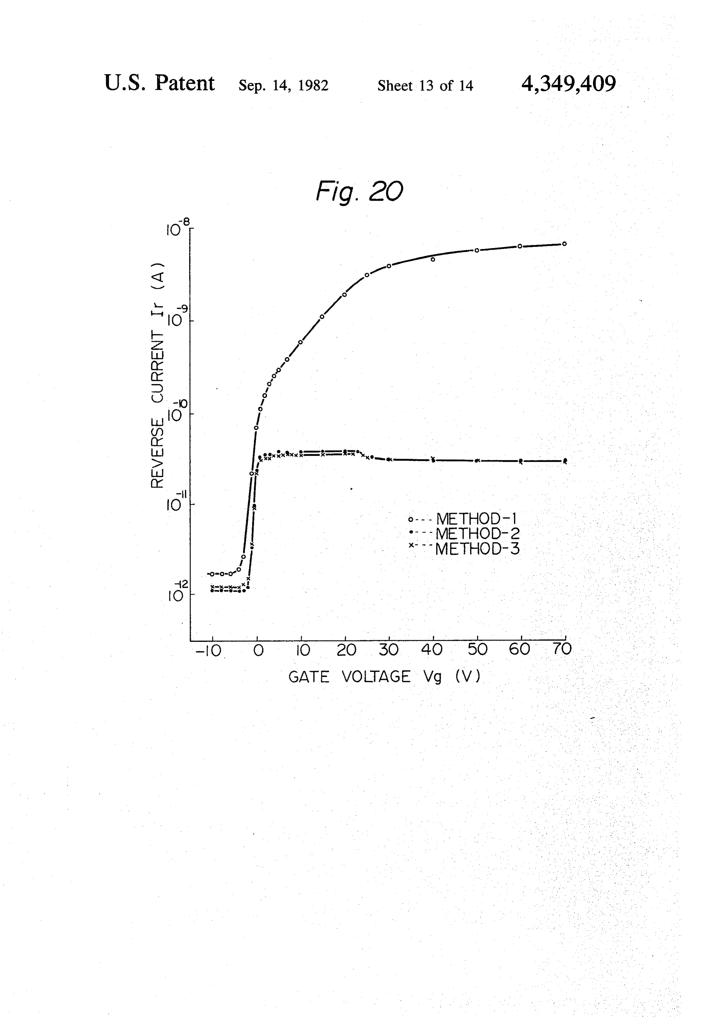
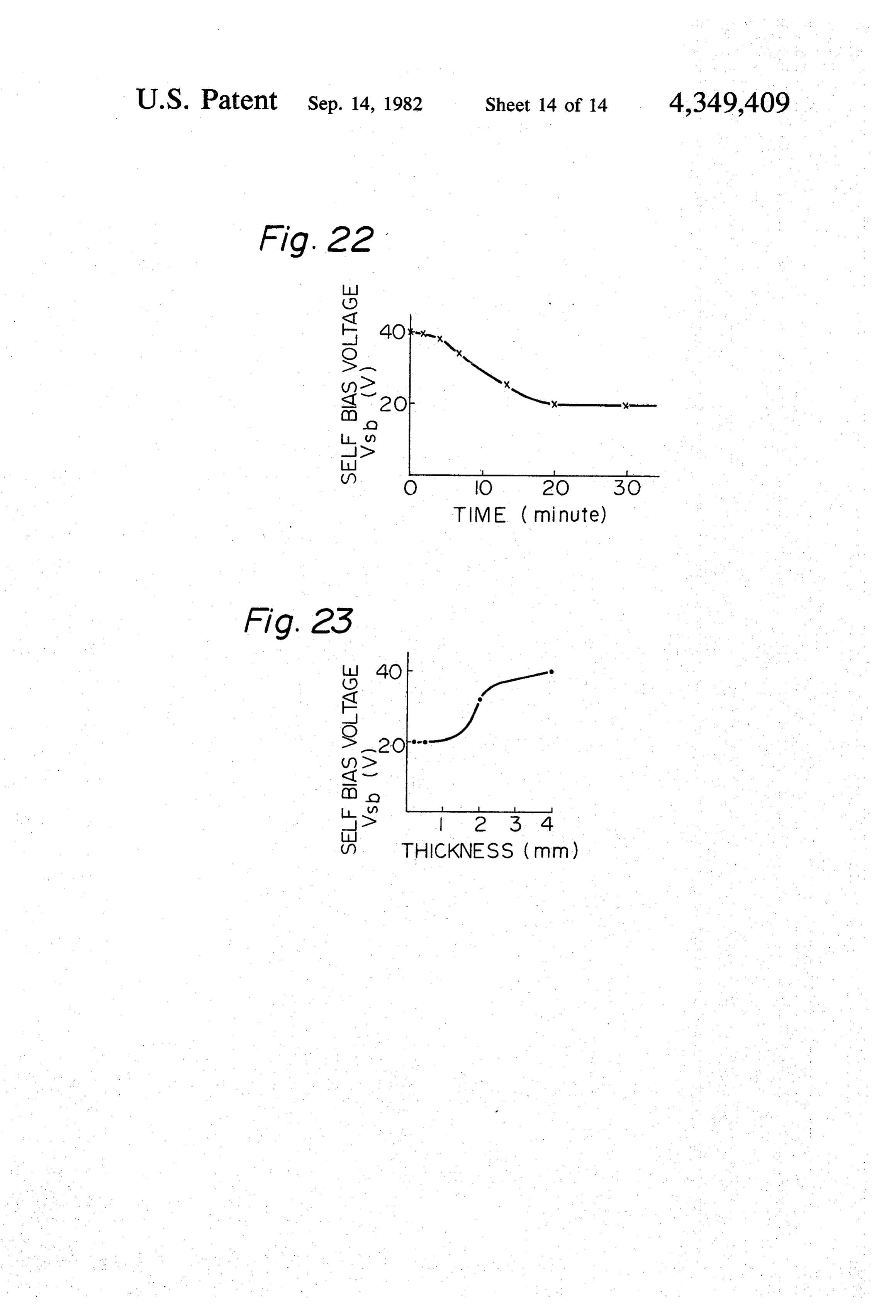
FIG. 23 illustrates the dependency of Vit upon the
Page 2drawing sheetscan →
Page 3drawing sheetscan →
Page 4drawing sheetscan →
Page 5drawing sheetscan →
Page 6drawing sheetscan →
Page 7drawing sheetscan →
Page 8drawing sheetscan →
Page 9drawing sheetscan →
Page 10drawing sheetscan →
Page 11drawing sheetscan →
Page 12drawing sheetscan →
Page 13drawing sheetscan →
Page 14drawing sheetscan →
Page 15drawing sheetscan →
Page 16scan →
however, is increased. According to the conventional
METHOD AND APPARATUS FOR PLASMA apparatus in which the position of the intermediate ETCHING electrode is fixed, it is not possible to maintain high
Background of the invention
selectivity while minimizing the damage due to the 5 processing.
1. Field of the Invention The present invention is proposed in order to solve The present invention relates to a method for effect the aforementioned problems inherent in the conven ing plasma etching for semiconductor materials and an tional art.
apparatus therefor. The method and apparatus accord The above mentioned conventional etching apparatus ing to the present invention can be used for the produc 10 has been disclosed in Japanese Patent Application No. tion of, for example, MOS type semiconductor inte 111257/78 (Japanese Patent Laid-Open No. 38043/80) grated circuits. that was filed by the inventors of the present invention. 2. Description of the Prior Art
In a parallel plate type plasma etching apparatus, SUMMARY OF THE INVENTION semiconductor elements are usually processed using a 15 The principal object of the present invention is to relatively high electric power of a high frequency in provide a method and apparatus for plasma etching order to attain fast etching speeds and good pattern specimens maintaining a high selectivity and etching edge profiles. Due to a capacitor in this case, a self-bias rate by continuously changing the bias voltage from a voltage is generated on a first electrode (for example, a high self-bias state to a low self-bias state by varying the cathode) on which is mounted a specimen of a semicon 20 gap between the intermediate electrode and the first ductor material that is to be processed. Owing to this electrode and by manipulating the RF power, wherein bias voltage, ions in the plasma are accelerated and the damaged layer (crystalline lattice disorder) intro impinge upon the specimen that is to be processed; i.e., products having excellent pattern edge profiles are ob duced into the specimen during the processing and tained. However, bombardment of high-energy ions 25 deposit on the processed surface, are sequentially re often damages the specimens that are to be processed. moved under the condition of a low self-bias voltage, The extent of the damage, usually, depends upon the and semiconductor elements having good electrical accelerating energy. From the standpoint of achieving characteristics can be obtained.
processing of a specimen without damage, therefore, it Another object of the present invention is to provide is desired to employ ions with a low accelerating en 30 a method and apparatus for plasma etching, which per ergy. Use of ions with a low accelerating energy, how forms a etching with increased stability and good repro ever, inevitably results in a decrease of the etching ducibility.
speed. To overcome this and to achieve the processing A further object of the present invention is to provide without any damage but with fast etching speed. There a method and apparatus for plasma etching, capable of has been proposed a particular device wherein, an inter 35 changing the etching rates of the materials to be pro mediate electrode, which serves as a third electrode, is cessed by applying a bias voltage to an intermediate provided in a generally employed two electrode type electrode.
plasma etching apparatus. According to one aspect of the present invention, FIG.1 illustrates a conventional apparatus for effect there is provided a method for effecting plasma etching ing plasma etching, having an intermediate electrode. of a specimen by using a first and a second electrode and Referring to FIG. 1, the apparatus consists of a first an electrically floated intermediate electrode, placing a electrode 1, a second electrode 2, a bell jar 3, a capacitor specimen on said first electrode and the electrically 5, a high frequency power supply 6, and an intermediate electrode 7. The intermediate electrode 7 has a shape of floated intermediate electrode, applying a high fre a disc and the disc has through holes. A specimen 4 is 45 to produce thebetween quency power said first and second electrode plasma between said first and second located on the first electrode 1.
The above mentioned apparatus was previously in electrode, and carrying out said etching under the con dition that the distance between said first and said inter vented by the inventors of the present invention. The inventors thereafter conducted further studies, and mediate electrodes is changed during said etching. According to another aspect of the present invention, found the facts as will be explained hereinbelow in the there is provided an apparatus for plasma etching com specification of this application, thus accomplishing the prising a first electrode, a second electrode, and an present invention. Namely, with the apparatus of FIG. electrically 1, the plasma density increases between the first elec floated intermediate electrode which is dis trode and the intermediate electrode and, hence, a high posed between said two electrodes, and wherein said etching rate is realized even at a low self-bias voltage, 55 apparatus further comprises a drive mechanism which and damage due to processing can be reduced. Such works to vary the distance between the intermediate effects are greatly dependent upon a gap between the electrode and the first electrode. intermediate electrode and the first electrode, and are. BRIEF DESCRIPTION OF THE DRAWINGS particularly striking when the gap is small. When, for example, SiO2 is to be processed for contact hole forma 60 FIG. 1 is a cross-sectional view illustrating the funda tion, however, a preferential etching of SiO2 to the mental construction of a conventional apparatus for underlying silicon cannot be performed. As the gap plasma etching; .. . .
between the intermediate electrode and the first elec FIG. 2A is a cross-sectional view illustrating the trode increases, on the other hand, the mode of dis fundamental construction of an apparatus which is em charge becomes similar to that of the two electrode 65 ployed for a method of plasma etching according to an type apparatus, whereby the self-bias voltage is in embodiment of the present invention;
creased and the processing causes increased damage. FIG. 2B is a perspective view illustrating an interme The selectivity of etching to the underlying silicon, diate electrode of the apparatus of FIG. 2A;
Page 17scan →
FIGS. 3 and 4 are views of intermediate electrodes DESCRIPTION OF THE PREFERRED according to another embodiment of the present inven EMBODIMENTS tion;
FIG. 5 and FIGS. 6A to 6C are views illustrating FIGS. 2A and 2B are diagrams illustrating an appara specific cases where a d.c. bias voltage is applied to the 5 tus used for the method of plasma etching according to intermediate electrode of FIG. 2A; an embodiment of the present invention. The apparatus FIGS. 7A to 7C are cross-sectional views illustrating for plasma etching comprises a first electrode 1, a sec the steps for forming fine contact holes in a semiconduc ond electrode 2, a bell jar 3, a capacitor 5, a high fre tor element according to the method of the present quency power supply 6, an intermediate electrode 7, invention; 10 and a drive mechanism 8, and subjects the surface of a FIGS. 8A to 8D are cross-sectional views illustrating specimen 4 to etching.
the steps for forming a PN diode by finely processing a The electric power of a high frequency is applied Si3N4 film according to the method of the present in between the first electrode 1 (cathode in this embodi vention; ment) and the second electrode 2 (anode in this embodi FIG. 9A is a plan view illustrating the construction of 15 ment) in the plasma etching apparatus from the high a test piece for comparing the contact resistances of frequency power supply 6 via capacitor 5, and a reac contact holes processed by a conventional method and tive gas, i.e., an active gas (such as CHF3, C2F6, C3F8, the method of the present invention;
FIG.9B is a cross-sectional view along the line B-B CF4+ H2, or the like) or an inert gas (such as argon, of FIG. 9A; 20 xenon, or the like), is introduced into the bell jar 3 of FIG. 10 is a histogram of contact resistances of the which the interior is maintained at a predetermined gas test pieces of FIG. 9A processed according to the con first and sosecond pressure, that a plasma discharge occurs between the electrodes. In this case, since there exists the intermediate electrode, the plasma is mostly
FIG.11 is a histogram like that of FIG. 10 but the test confined pieces being processed according to the method of the 25 ate electrode. between the first electrode and the intermedi present invention; The intermediate electrode 7 consists of a FIG. 12 is a histogram of breakdown voltages of PN trated circular plate having many through holes 71 as illus diodes which were processed by a wet chemical etching discharge in a perspective view of FIG. 2B. As the plasma in the steps of FIGS. 8A to 8D; occurs, a negative self-bias voltage is gener ated on the first electrode 1 due to the capacitor 5.
* FIG. 13 is a histogram of breakdown voltages of PN 30 Therefore, diodes which were processed by the conventional the surface ions in the plasma are accelerated to subject of the specimen 4 to etching. The energy of method in the steps of FIGS. 8A to 8D;
FIG. 14 is a histogram of breakdown voltages of PN ions impinging upon the specimen is determined by the diodes which were processed by the method of the self-bias voltage; the energy increases with the increase present invention in the steps of FIGS. 8A to 8D; 35 in the self-bias voltage. The drive mechanism 8 so . . FIG. 15 is a diagram illustrating relations between the works that a distanced between the intermediate elec RF power and the self-bias voltage in the apparatus of trode 7 and the first electrode 1 can be changed exter FIG. 2A; nally of the bell jar 3 side. FIG. 16 is a diagram illustrating relations between the FIGS. 3 to 5 illustrate modified examples of the inter self-bias voltage and the gap between the intermediate 40 mediate electrode of FIGS. 2A and 2B equipped with electrode and the first electrode of the apparatus of the drive mechanism. Referring to FIG. 3, the interme FIG. 2A with the RF power as a parameter; diate electrode 7 is equipped with spacers 72 which are FIG. 17 is a diagram showing the depth profile of made of an insulating material such as Al2O3 or a mate carbon from the surface of the silicon substrate pro rial having electric resistance. If the thickness 1 of the cessed by each of three processing methods; 45 spacer 72 is so set that the intermediate electrode 7 FIG. 18 is a diagram illustrating the lattice defects in exhibits optimal effects, it is possible to accurately main the silicon substrate processed by each of the processing tain the distance d when the spacers 72 come into methods, as analyzed by the Het Rutherford back-scat contact with the first electrode. - tering method; FIG. 4 illustrates the intermediate electrode 7 having FIG. 19 is a cross-sectional view illustrating the con 50 electrically conductive support rods 73 on the upper struction of a gate-controlled diode which is used as a portion thereof. When the intermediate electrode is test device for measuring electrical characteristics of raised, the support rods come into contact with the the specimens processed by each of the processing second electrode. With the support rods being made of methods; an electrically conductive material, the second elec FIG. 20 is a diagram illustrating the reverse currents 55 trode becomes electrically conductive to the intermedi of a gate-controlled diode processed by each of the ate electrode. Therefore, the intermediate electrode acts processing methods; as the second electrode, and the discharge takes place FIG. 21 is a diagram showing the relation between between the intermediate electrode and the first elec the RF power and the self-bias voltage when the inter trode. In this case, the mode of discharge is the same as mediate electrode in the apparatus of FIG. 2A has a 60 that of the conventional two electrode type plasma thickness of 4 mm; etching apparatuses even when the gap is narrow be FIG. 22 is a diagram illustrating the change of the tween the intermediate electrode and the first electrode, self-bias voltage in the apparatus of FIG. 2A with re and the distance for moving the intermediate electrode spect to the passage of time; and can be reduced.
FIG. 23 is a diagram illustrating the dependency of 65 FIG. 5 illustrates an embodiment, in which a voltage the self-bias voltage in the apparatus of FIG. 2A upon is supplied to the intermediate electrode 7 from an ex the thickness of the intermediate electrode when the ternal unit to change the processing conditions. The discharge is being initiated. . - voltage is supplied from an external d.c. power supply
Page 18scan →
91 to the intermediate electrode 7 via a circuit consist entitled “Gap between the First Electrode and the In ing of an inductor 93 and a capacitor 92. termediate Electrode' set forth hereinafter. . In FIG. 5, the intermediate electrode 7 is served with The above mentioned etching for the SiO2 layer on a voltage from the external power supply. FIGS. 6A to the silicon semiconductor substrate is employed for 6C illustrate specific examples in which a d.c. voltage is forming fine contact holes in such devices as MOS applied to the intermediate electrode 7 by utilizing a integrated circuits.
negative self-bias voltage Vb which is induced in the FIGS. 7A to 7C illustrate the steps for forming fine . first electrode 1 during the discharge, without utilizing contact holes. First, a silicon dioxide layer 42 is depos the external power supply. Referring to FIG. 6A, a ited on a silicon substrate 41, and a predetermined por resistor R1 is connected between the second electrode 2 10 tion is removed by etching as shown in FIG. 7A. An and the intermediate electrode 7, a resistor R2 is con arsenic implanted layer 45 is formed in the silicon as nected between the intermediate electrode 7 and the shown in FIG. 7B, and onto which is formed a silicon first electrode 1, and resistances of the resistors are dioxide film 44 or PSG (phosphosilicate glass) by chem selected to be sufficiently smaller than the impedances 15 ical vapor deposition (CVD) method. The film 44 is ZP1, ZP2 of the plasma (R1<<ZP1, R2 <<ZP2). The then subjected to the selective etching in accordance potential Vie of the intermediate electrode 7 is then resist the with method of the present invention through a film 43 as shown in FIG. 7B, in order to obtain a
CVD SiO2 film 44 as shown in FIG. 7C. Aluminum
Vie= R1/(R--R2)Wt, (1) electrodes 46, are formed in the holes formed in the 20 CVD SiO2 film by the etching.
Thus, it is possible to obtain a potential which is deter It is also possible to provide a step of incineration mined by the resistances. When the resistances R1, R2 treatment using oxygen plasma in the processing steps are nearly equal to the plasma impedances ZP, ZP2, of Example 1, in order to incinerate the resist film. the impedances. ZP1, ZP2 are not negligible, and the 25 EXAMPLE 2 potential Vie is not given by the equation (1). In this case, however, it is possible to eliminate either one of Below is mentioned an example in which a silicon semiconductor material the resistors R1 or R2 as shown in FIG. 6B or 6C, by thickness of 1000 angstroms having an Si3N4 layer of a utilizing the impedances ZP and ZP2. on the substrate, is sub Below are mentioned the steps for plasma, etching 30 jected to etching.
First, the Si3N4 layer is removed by etching which according to the present invention.
continued for about 4 minutes under the conditions of
EXAMPLE 1. using an intermediate electrode of a thickness of 0.5
Below is mentioned an example. in which a silicon mm, distance d of 48 mm, RF power of 200 watts, and semiconductor material having a SiO2 layer of a thick 35 pressure550of volts, in the presence of CHF3 gas at the
Pa. The over-etching is further contin ness of 8000 angstroms on the substrate, is subjected to ued for about 1 minute (etching of the first stage).
First, the intermediate electrode 7 having a thickness After the above etching has been finished, the dis of 0.5 mm is brought into contact with the second elec tance d is adjusted to 16 mm by the up/down drive mechanism, and the surface is treated for 10 minutes trode 2 by the up/down drive mechanism 8, or the under the conditions of RF power of 25 watts and Vi, distanced between the intermediate electrode 7 and the of 20 volts in the presence of a CF4+20%O2 gas at the first electrode 1 is maintained to be greater than 48 mm. pressure of 1.33 Pa (etching of the second stage). Then, the silicon dioxide layer is subjected to the etch After the above treatment is finished, the distance d is ing under the conditions of RF power of 200 watts, Vs, reduced to less than 5 mm to discontinue the etching. of 550 volts, in the presence of CHF3 gas at a pressure 45 The above mentioned etching for the Si3N4 layer on of 1.33 Pa (0.01 Torr) for about 25 minutes. Then, over the silicon semiconductor substrate is employed for etching is performed for about 5 minutes to completely finely processing the Si3N4 film in the steps of forming remove silicon dioxide (the etching of the first stage). PN diodes. FIGS. 8A to 8D illustrate the steps for After the above step has been finished, the intermedi forming PN diodes. First, an Si3N4 film 402 on a silicon ate electrode 7 is set to a distanced, which is suitable for 50 substrate 401 is processed by the method of the present exerting the effect of the intermediate electrode, for invention using a resist layer 403 as an etching mask, to example, 16 mm by the drive mechanism 8, and the obtain the Si3N4 film 402 as shown in FIG. 8B. Then, an surface is cleaned under the conditions of RF power of SiO2 film 404 is formed by selective oxidation. After the 25 watts, Vsh of 20 volts, in the presence of Si3N4 film has been removed, arsenic ions are implanted CF4-20%O2 gas at the pressure of 1.33 Pa for 10 min 55 into the silicon substrate, and an arsenic ion implanted utes (the etching of the second stage). In this case, the layer 405 is formed by heat treatment thereby to obtain silicon surface is etched to a depth of 100 angstroms. a PN diode. - This dry-cleaning of the surface removes damage in the EXAMPLE 3 processed surface and contamination composed of the polymer film. . . . '. 60 . In this example, a voltage is applied to the intermedi After the above cleaning has been carried out, the ate electrode from an external unit. This makes it possi gap d between the intermediate electrode.7 and the first ble to change the processing conditions, particularly the electrode 1 is reduced to be smaller than 5 mm by the etching selectivity. The following Table shows etching drive mechanism 8. Thus the discharge between the rates for various materials. As a reactive gas, intermediate electrode 7 and the first electrode 1 com 65 CF4+5%O2 gas at a pressure of 1.33 Pais used, and the pletely ceases, and the etching is stopped. Experimental etching is performed at an RF power of 100 watts: results related to a gap between the first electrode and Numerals in the parentheses represent ratios of the the intermediate electrode are disclosed in the section etching rate for silicon. . ."
Page 19scan →
TABLE Contamination and Lattice Defect on the silicon surface voltage applied to the etching rate (angstrons/min) intermediate electrode (V) Si3N4 SiO2 Si
FIGS. 17 and 18 illustrate the results of the two stage processes of the aforementioned Examples 1 and 2.
O 460(1.6) 220(0.8) 290(1) 5 Namely, FIG. 17 shows the contamination on the sili -- 0:0 300(1.7) 120(0.7) 180(1) con surface after the CVD SiO2 film and Si3N4 film have been etched, which is measured by X-ray photoe lectron spectroscopy (XPS). A polymer film composed
When a voltage of + 100 volts is applied to the inter of carbon and fluorine is formed on the surface of the mediate electrode, the etching rate becomes low for all 10 silicon after the CVD SiO2 film or Si3N4 film is etched of the materials. The ratios of the etching rate of Si3N4 by the first stage etching. FIG. 17 illustrates the depth and SiO2 to silicon, however, do not change. When a profile of carbon from the surface of the silicon, in voltage of -100 volts is applied, on the other hand, the which the abscissa represents the etching time (minutes) etching rate becomes low, particularly for silicon. Con by argon ions (Art) during the XPS analysis, and the sequently, the ratios of etching rate of SiO2/Si and 15 ordinate represents the peak height (arbitrary unit) of Si3N4/Si become high. In particular, the ratio of the carbon.
etching rate of Si3N4/Si is increased by 4.1 times. With METHOD-1 represents the data of XPS analysis a usual parallel plate type plasma etching apparatus which is carried out after the CVD SiO2 film is sub using CF4-5% O2 gas, the ratio of Si3N4 to silicon is jected to the first stage etching. METHOD-2 represents low. The ratio, however, can be increased by using an 20 the data obtained from the specimen which is subjected intermediate electrode and by applying a negative d.c. to the second stage etching for 10 minutes using the bias voltage thereto. apparatus having the intermediate electrode after the first stage etching has been performed in accordance
Gap between the First Electrode and the Intermediate 25 with the present invention, and METHOD-3 represents Electrode the data obtained from the specimen which is etched by FIG. 15 illustrates a relation between the RF power wet chemical etching.
and the self-bias voltage in the parallel plate type plasma According to FIG. 17, large amounts of carbon are etching apparatus having an intermediate electrode. In deposited on the silicon surface when the CVD SiO2 this case, the reactive gas is CF4-20%O2 gas at a pres 30 film is subjected to the first stage etching, as compared sure of 1.33 Pa (0.01 Torr). with the wet etching method. However, when the sili In FIG. 15, symbol d denotes the distance between con substrate is subjected to the second stage etching the intermediate electrode and the first electrode. The after the first stage etching using the apparatus having intermediate electrode has a thickness of 0.5 mm. Under an intermediate electrode, the peak height of carbon is the condition that the values of RF powers are the decreased to the same level as that in METHOD-3.
same, the self-bias voltage Vist, can be reduced in the FIG. 18 illustrates the results of the surface analysis case where an intermediate electrode is provided, the comparingusing the He Rutherford backscattering method for smaller the distance d is, the greater the effects are. The plasma the lattice defect of crystals induced by the curve indicated as NIE represents the case when there etching. Processing conditions of the designated is no intermediate electrode. The broken curves indi 40 METHOD-1 to METHOD-3 are the same as those of cated as 10 A/min, 50 A/min and 100 A/min denote the aforementioned XPS methods 1, 2, and 3. Small lines on which the etching rates for silicon are 10 A/- squares represent analytical results from random direc min, 50 A/min, and 100 A/min, respectively. Accord tions, which are reference values of the Rutherford backscattering method. According to this method, at a ing to FIG. 15, the self-bias voltage V.sb can be reduced backscattered at the same RF power without decreasing the etching 45 scattering energy of about 0.84 MeV in the back rate for silicon. spectra, 500 counts of surface peak is mea sured after the CVD SiO2 has been subjected to the first
FIG. 16 illustrates the dependency of the self-bias stage etching compared to 300 counts in the wet chemi voltage Vs, upon the distance between the intermediate cal etching, electrode and the first electrode with the RF power 50 defect of siliconand this indicates the presence of a lattice (Pri) as a parameter. As the distance is reduced, the high self-bias voltagenear the surface due to processing at a self-bias voltage Vb is reduced under all of the RF second stage, however, Vsb. Through the etching of the power conditions. When the distance is extremely re nearly equal to that of thethe surface peak becomes duced, however, the discharge becomes unstable or is that the lattice defect is removed.etching, wet which means
In FIG. 18, the ab interrupted between the intermediate electrode and the 55 scissa represents the backscattered energy (MeV) and first electrode. Hatched areas in FIGS. 15 and 16 repre the ordinate represents the backscattered counts per sent the regions where the discharge becomes unstable channel.
between the intermediate electrode and the first elec trode, where the discharge is interrupted, or where the Contact Resistance discharge takes place between the intermediate elec 60 FIGS. 9A and 9B illustrate the construction of a test trode and the second electrode but does not take place piece for measuring the contact resistance of the contact between the intermediate electrode and the first elec holes which are processed by the conventional etching trode. This is attributed to the development of dark method and the method of the present invention. FIG. space in which an intense electric field is concentrated 9A is a plan view of the test piece, and FIG. 9B is a near the first electrode in the plasma. In this case, if the 65 cross-sectional view along the line B-B of FIG. 9A. intermediate electrode is brought too close to the first The size of the contact hole is 33x3 m2. The test piece electrode, the intermediate electrode is connected to the consists of aluminum electrodes 406, an SiO2 layer 407, first electrode presumably through the dark space. and an arsenic implanted layer 408.
Page 20scan →
FIG. 10 is a histogram of contact resistance of the which the Si3N4 film on the silicon substrate is subjected contact holes which are formed according to the con to etching of the first stage only. METHOD-2 repre ventional method, i.e., by the etching of the first stage sents the result obtained by the process in which the only. Namely, the contact hole is formed by dry pro etching of the second stage is effected for 10 minutes at cessing using CHF3 as the reactive gas at a self-bias a low self-bias voltage according to the method of the voltage Vsh of 550 volts. present invention. METHOD-3 represents the result of FIG. 11 is a histogram of contact resistance of the the diode which is fabricated by the wet etching contact holes which are formed according to the method. The effect of the method according to the method of the present invention. In this case, the SiO2 present invention is comparable to that in the conven film of a thickness of 8000 angstroms is subjected to 10 tional wet chemical etching. With the etching of the etching for about 25 minutes under the conditions of a first stage only, however, reverse current Iris increased. thickness of the intermediate electrode of 0.5 mm, dis This is presumably due to the presence of a lattice de tance d of 48 mm, RF power of 200 watts, self-bias fect and polymer film on the processed surface, which voltage Vs, of 550 volts, using a CHF3 gas at a pressure acts as the generation-recombination (g-r) center. of 1.33 Pa, followed by over-etching for about 5 min 15 According to the present invention as mentioned utes. It is further subjected to etching for 10 minutes by above, the etching of the second stage gives distin adjusting the distanced to 16 mm, using CF4-20%O2 guished effects without causing damage to the specimen gas at a pressure of 1.33 Pa under the conditions of RF being processed like the wet chemical etching, or with power of 25 watts and the self-bias voltage of 20 volts. out deposits on the processed surfaces. Comparison of FIG. 10 with FIG. 11 indicates that 20 when the etching of the second stage is performed by Experiments related to the Thickness of the adjusting the distanced to 16 mm as contemplated by Intermediate Electrode the present invention, variance in the contact resistance The aforementioned embodiments of FIGS. 2A to 6C is reduced and the contact resistance is decreased. did not particularly deal with the thickness of the inter 25 mediate electrode. According to the study conducted
Reverse characteristics of PN Junction
FIGS. 12 to 14 are histograms of breakdown voltages by the inventors of the present invention, however, it was determined that the thickness of the intermediate of PN diodes which are formed by finely processing the electrode affects the stability of the discharge. Below Si3N4 film. FIG, 12 represents the result in which PN are mentioned relations of various conditions such as diodes were processed by the wet chemical etching 30 RF power relative to the self-bias voltage V. using hot phosphoric acid. FIG. 13 is a histogram of FIG. 21 illustrates a relation between the RF power breakdown voltages of PN diodes which were fabri and the self-bias voltage Vsh in case of the intermediate cated by the conventional method without the etching electrode with a thickness of 4 mm. The distance be of the second stage. FIG. 14 represents, the result ob tween the intermediate electrode and the first electrode tained by the fabrication process in which the Si3N4 film 35 is 16 mm. There is a difference between the state where of a thickness of 1000 angstroms on the silicon substrate the discharge is being initiated and the state where the is subjected to plasma etching of the first stage for about discharge is stably sustained when the self-bias voltage 4 minutes in accordance with the method of the present Vsh is lower than 100 volts. Such phenomenon, how invention under the conditions of a thickness of the ever, is not observed when the intermediate electrode intermediate electrode of 0.5 mm, distance d of 48 mm, 40 has a thickness of 0.5 mm. - RF power of 200 watts, and self-bias voltage Vh of 550 FIG. 22 illustrates the change of Vsh with the passage volts, using a CHF3 gas at a pressure of 1.33 Pa, fol of time when the discharge is maintained at an RF lowed by over-etching for about 1 minute and then is power of 25 watts. The distance is 16 mm between the further subjected to the etching of the second stage by intermediate electrode and the first electrode. The self adjusting the distanced to 16 mm, using CF4-20%O2 45 bias voltage Vst, is high when the discharge is initiated; gas at a pressure of 1.33 Pa under the conditions of RF about 20 minutes are required for assuming a stable Vsb. power of 25 watts and Vb of 20 volts. The breakdown Under such conditions, the Vsh undergoes the change voltage of any PN diode processed according to the while the specimen is being processed, and it is difficult method of the present invention is greater than 30 volts, to obtain a predetermined etching rate maintaining unlike that processed by wet etching. 50 good reproducibility. The thickness of the intermediate Experiments using Gate-Controlled Diode electrode, in this case, is 4 mm.
FIG. 23 illustrates the dependency of Vit upon the
The effects of the present invention were investigated thickness of the intermediate electrode when the dis in detail by the inventors using a gate-controlled diode, charge is initiated. The RF power is 25 watts, and the similar to the case of the above described PN diode. 55 distance is 16 mm between the intermediate electrode FIG. 19 illustrates the construction of the gate-con and the first electrode. As the thickness of the interme trolled diode. A gate voltage Vg and a reverse voltage diate electrode becomes greater, the self-bias voltage V, are applied to aluminum electrodes 411 and 412, Vs, in the beginning of the discharge relative to Vsh respectively. Aluminum electrode 411 as a gate elec under stable conditions become higher. When the thick trode is located on an SiO2 film 413 and arsenic ions are 60 ness is reduced to less than 2 mm, the Vs in the begin implanted into a p-type silicon substrate 415 and the ning of the discharge becomes equal to the Vish under specimen is annealed to form an n-type arsenic im stable conditions. Consequently, it is recommended to planted layer 414. reduce the thickness of the intermediate electrode to FIG. 20 illustrates the relation between the gate volt less than 2 mm.
age Vg and the reverse current I, of the gate-controlled 65 We claim:
diode. In this case, the reverse voltage V, is 15 volts. In 1. A method for effecting plasma etching of a semi FIG. 20, METHOD-1 represents the characteristic of conductor material comprising the steps of providing a the gate controlled diode fabricated by the process in first and a second electrode and an electrically floating 21 intermediate electrode, placing a semiconductor mate C2F6, C3Fs, and CF4+ H2, and in the additional etching rial on said first electrode and said electrically floated the second reactive gas is CF4--O2. intermediate electrode, applying a high frequency 8. The method of claim 6 or 7, wherein the pedeter power between said first and second electrode to pro mined distance between the intermediate electrode and duce a plasma between said first and second electrode, 5 the first electrode in the initial etching is set at approxi and etching the semiconductor material under the con mately 48 mm. or more.
dition that the distance between said first and said inter 9. The method of claim 6 or 7, wherein the thickness mediate electrode is changed during said etching. of the intermediate electrode is less than 2 mm. 2. A method as set forth in claim 1, wherein the semi 10. The method of claim.8, wherein the thickness of conductor material is processed under the conditions of 10 the intermediate electrode is less than 2 mm. a high input power and a high self-bias voltage while maintaining a predetermined distance between the in first11. electrode,
An apparatus for plasma etching comprising a a second electrode, an electrically termediate electrode and the first electrode, then said floated intermediate distance is reduced to be smaller than said predeter two electrodes, and aelectrode positioned between said mined distance, and the semiconductor material is fur 15 distance between saiddrive mechanism for varying the intermediate electrode and said ther processed under the conditions of a low input first electrode.
power and a low self-bias voltage. 12. An apparatus for plasma etching as set forth in 3. A method as set forth in claim 1 or 2, wherein the semiconductor material is subjected to the etching claim 11, iswherein the thickness of said intermediate while continuously changing the distance between said 20 electrode smaller than 2 mm. 13. The apparatus of claim 11, wherein said interme intermediate electrode and said first electrode.
4. A method as set forth in claim 1 or 2, wherein a diate electrode has spacers formed of an insulating ma voltage from an external source is applied to said inter terial, facing the first electrode, and with a thickness for maintaining a predetermined distance between the first mediate electrode.
5. A method as set forth in claim 1 or 2, wherein the 25 and14.intermediate
The electrodes.
apparatus of claim 11 or 13, wherein said distance between said intermediate electrode and said first electrode is set to a predetermined length, said high intermediate electrode has electrically conductive sup frequency power is set to a predetermined value, and port rods facing the second electrode, wherein the sec wherein the semiconductor material is subjected to a ond electrode becomes electrically conductive to the intermediate electrode when the support rods contact first etching using a first reactive gas, the distance be the second electrode.
tween said intermediate electrode and said first elec trode is then reduced to be smaller than said predeter 15. The apparatus of claim 11, further comprising a mined length, the high frequency power is set to a value housing for containing said first, second, and intermedi which is smaller than said predetermined value, and the ate electrodes and introducing an etching plasma semiconductor material is subjected to an additional 35 therein.
etching using a second reactive gas. 16. The apparatus of claim 15, further comprising 6. A method as set forth in claim 5, wherein the semi means external of said housing for supplying a voltage conductor material comprises a substrate and a SiO2 to the intermediate electrode.
layer and wherein in the first etching the SiO2 layer is 17. The apparatus of claim 15, further comprising removed using a first reactive gas selected from CHF3, means internal of said housing for supplying a voltage C2F6, C3Fs, and CF4--H2, and in the additional etching to the intermediate electrode.
the second reactive gas is CF4-O2. 18. The apparatus of claim 17, wherein said internal 7. A method as set forth in claim 5, wherein the semi voltage supplying means comprises at least one resistor conductor material comprises a substrate and a Si3N4 connected between the intermediate and first electrodes layer and wherein in the first etching the Si3N4 layer is 45 or between the intermediate and second electrodes. removed using a first reactive gas selected from CHF3, s
Page 22scan →
United states patent and trademark office
Certificate of correction
INVENTOR(S) : Shibayama et al.
It is Certified that error appears in the above-identified patent and that said Letters Patent is hereby corrected as shown below:
Front page, 57) ABSTRACT, line 4, "state" should be
Col. l. line 34 , "speed. There" should be --speed, there--.
line 42, delete "and the electrically";
line 43, delete "floated intermediate electrode". 4, line 38, delete "side".
10 line 59, "become" should be --becomes --.
eigned and Sealed this
Twenty-fifth D 2 y of June 1985
Seal)
Donald j. qugg
Attesting Officer Acting Commissioner of Patents and Trademarks
Page 23scan →
United states patent and trademark office
Certificate of correction
INVENTOR(S) : Shibayama et al.
It is certified that error appears in the above-identified patent and that said Letters Patent is hereby corrected as shown below:
column ll, line 2, delete "and said electrically floated"; line 3, delete "intermediate electrode".
eigned and Scaled this
Fourth O 2 y of February 1986
Seal
Attest:
Donald j. quigg
Attesting Officer Connissioner of stents and Trademarks
Provenance
- Collection
- Patents citing this work
- Pages
- 23
- Method
- pdftotext (the PDF's own text layer) + pdftoppm 300dpi page scans
- Patent office record
- patents.google.com →
- Source
- Google Patents citing-documents table
- Assignee
- Fujitsu Limited
- Published
- 1982-09-14
- Transcribed from
- patentimages.storage.googleapis.com →