

patent · US4353777A
Selective plasma polysilicon etching
12 October 1982
Text
Page 1bibliographic recordscan →
United States Patent (19) 11 4,353,777 Jacob Oct. 12, 1982 54 SELECTIVE PLASMA POLYSILICON 4,162,185 7/1979 Coburn et al. ...................... 156/643 ETCHING 4,162,210 7/1979 Deppe .......... ... 204/192 4,180,432 12/1979 Clark ... ... 156/643 75 Inventor: Adir Jacob, Framingham, Mass. 4,182,646 1/1980 Zajac ........ ... 156/643 4,188,426 2/1980 Auerbach .............................. 427/40 (73) Assignee: LFE Corporation, Clinton, Mass. 4,190,488 2/1980 Winters ........ ... 56/643 21 Appl. No.: 255,495 4,203,800 5/1980 Kitcher et al. ... 156/643 4,209,356 6/1980 Stein ................. ... 156/643 22 Filed: Apr. 20, 1981 4,23,818 7/1980 Lemons et al. .. ... 156/643 51 Int. Cl. ........................................... H01L 21/306 4,214,946 7/1980 Forget et al. .... ... 56/643 4,229,247 10/1980 Chiu et al..... ... 156/643 52 U.S. C. .................................... 156/643; 156/646; 4,233,109 11/1980 Nishizawa .... ... 156/643 156/657; 156/659.1; 156/345; 204/192 E; 4,253,907 3/1981 Parry et al... ... 56/643 204/298; 252/79.1 4,255,230 3/1981 Zajac ........ ... 156/643 Field of Search ............... 156/643, 646, 657, 662, 4,298,443 11/1981 Maydan ............................... 204/192 156/659.1, 345; 204/192 E, 164, 192 EC, 298; OTHER PUBLICATIONS
References Cited Japan. J. Appl. Phys. Suppl. 2, Pt. 1, 1974, RF Sputter Etching by Fluoro-Chloro-Hydrocarbon Gases by
Re. 30,505 2/1981 Jacob ................................... 56/643 LFE Corporation, Plasma Systems, Bulletin 8277-PB1 3,654,108 4/972. Smith, Jr. ... 204/164 dated Feb. 1979.
3,806,365 4/1974 Jacob ...................................... 134/ 3,880,684 4/1975 Abe ......................................... 156/8 Primary Examiner-William A. Powell 3,940,506 2/1976 Heinecke ... 427/38 Attorney, Agent, or Firm-Kenway & Jenney 3,951,709 4/1976 Jacob ...................................... 156/8 3,951,843 4/1976 Jacob ......... ... 252/187 R. 57 ABSTRACT 3,975,252 8/1976 Fraser et al. ........................ 204/192 A process for etching polysilicon material preferentially 3,984,301 10/1976 Matsuzaki et al. ... 204/192 4,028,155 6/1977 Jacob .............. ... 156/643 over silicon oxide. The process is anisotropic and em 4,066,037 /1978 Jacob ...... 18/49.1 ploys a moderate to low pressure of Freon 11 (CFCl3) 4,069,096 1/1978 Reinberg et al. .. ... 56/643 in an RF plasma discharge. In a second embodiment 4,073,669 2/1978 Heinecke et al. .. ... 156/643 helium is mixed with the Freon 11 to inhibit degradation 4,094,732 6/1978 Reinberg........ ... 156/643 of the photoresist mask.
4,123,564 10/1978 Ajima ......... ... 427/85 4,123,663 10/1978 Horiike ............................... 250/531 4,148,705 4/1979 Battey et al..................... 204/192 E 6 Claims, 1 Drawing Figure
GEN
OLTP
xxYxxxxx xxxx
vAcjuM
PUMP
Drawings
Page 2drawing sheetscan →
Page 3scan →
polysilicon with respect to the etch rate of the underly
SELECTIVE PLASMA POLYSLICON ETCHING ing silicon oxide to provide enough control during the etching for the preservation of thin and ultrathin silicon
FIELD OF THE INVENTION oxide dielectric underlayers in field effect devices. This invention relates in general to fabrication of It is therefore a primary object of the present inven semiconductors and more particularly to a plasma etch tion to provide a plasma etching technique for utiliza ing technique for etching of polycrystalline silicon tion during semiconductor fabrication in which highly (polysilicon). efficient polysilicon etching takes place with a high BACKGROUND OF THE INVENTION degree of selectivity with respect to the etching of sili 10 con oxide, and wherein highly anisotropic etching takes
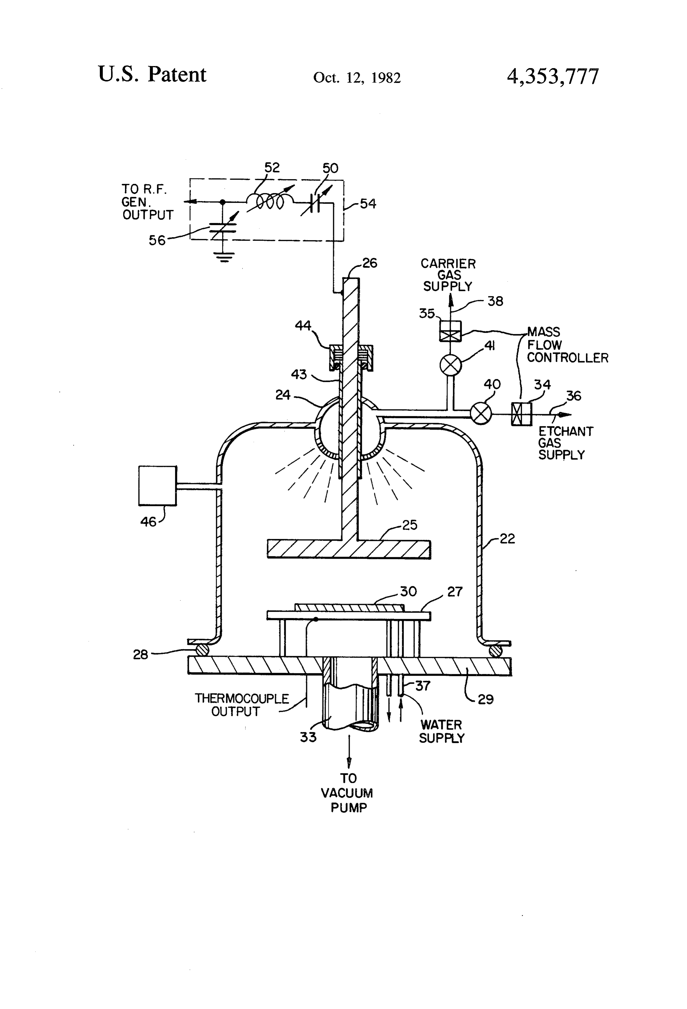
The manufacturing of semiconductor devices and place to provide substantially vertical profiles in the related thin film circuitry usually involves etching of features etched in the polysilicon layer, where the re specific layers comprising the device. Typically, the moval process is primarily due to chemical interactions area to be etched is masked by material such as photore 15 and is void of adverse radiation damage effects. sist with the mask forming a pattern of lines and areas SUMMARY OF THE INVENTION exposing the layer to be etched. In earlier approaches, the etching was carried out by a wet chemical method Broadly speaking, in the present invention, the gas in which the etchant material, typically oxidizing min plasma consists essentially of RF-discharged Freon 11 eral acids, contacted the exposed surface. (CFCl3) employed at moderate to low pressures, typi More recent processes employ gas plasmas, particu 20 cally 100 micron Hg, for highly efficient and uniform larly fluorine based gases selected from the saturated anisotropic etching of polysilicon. The process is highly halocarbon series, which eliminate some of the undesir able effects of wet chemistry. However, in both meth selective for polysilicon with respect to silicon oxide and produces substantially vertical etched profiles for ods the etching was basically isotropic. With isotropic features etching random etching proceeds at a uniform rate in all 25 (typicallyinone the range of submicron to a few microns to four microns). In one embodiment the directions. As the surface to be etched is removed, the addition of helium gas to Freon 11, to form a binary etching action takes place not only vertically into the gaseous mixture before surface, but also horizontally against the edge of the fects the photoresist masktheduring discharge, beneficially af. etching because of its recess created by the etching. Thus, the area to be high heat transfer property and the prevention of hot etched suffers undercutting in which the material is 30 spot formation. This results in insignificant degradation etched not only vertically in line with the edge of the opening in the photoresist mask, but also it extends of the photoresist during etching of polysilicon without significantly affecting the average etch rate of the underneath the photoresist mask. Typically this under polysilicon itself. This etching technique may be em cutting extends horizontally in substantially the same degree as the vertical etching. 35 ployed with both batch and in-line systems for the pro As the trend toward miniaturization continues, scal cessing of semiconductor devices and is also suitable for ing down to the micron and submicron dimension re etching of metal silicides overcoating polysilicon. Sili gions becomes a reality. This imposes strict demands on cides of titanium, tantalum, molybdenum and tungsten etch profiles, characteristically in the direction of verti are good candidates for such a process. cal etch profiles with insignificant undercutting. This DESCRIPTION OF THE DRAWING mode of plasma etching, commonly referred to as aniso tropic etching, is the result of directional effects that In the drawing, suppress isotropic etching. Ideally, it provides for a FIG. 1 is an illustration in diagrammatic form of an vertical etch wall on a plane closely approximating that apparatus suitable for use in the practice of this inven delineated by the resist edge prior to the etching opera 45 tion.
tion.
As techniques of lithography improve, line patterns DESCRIPTION OF PREFERRED of micron and submicron dimensions in photoresist EMBODIMENTS images become possible. In order to effectively transfer In the FIGURE there is illustrated an apparatus suit these images to the various substrates, reliable, repro 50 able for use in the process of the invention. The reactor ducible anisotropic etching is necessary. In the past, in chamber 22 is generally cylindrical in shape, is typically order to compensate for the undercutting effect of iso formed of quartz or other type of suitable glass and is tropic etching, the line width in the mask was made sealed through O-ring 28 to a base plate 29, which narrower than the desired line width in the layer to be would usually also be formed of quartz. At the top of etched, anticipating the widening of the line resulting 55 reaction chamber 22 a coaxial gas dispersion jet ar from undercutting. With the demand for much smaller rangement 24 allows gas to enter the reaction chamber. dimensions of line width and spaces, the lack of control A generally disk shaped and temperature controlled and reproducibility resulting from undercutting, has water cooled electrode 25 is carried on a supporting rod made isotropic etching unacceptable. 26 and is adjustably positioned from the top of the reac Other prior art techniques have employed reactive tor through electrode guide 43 and frictional coupling ion etching performed at low pressure. However, while 44. A suitable material for this electrode 25 is aluminum. this technique can produce some anisotropically etched The semiconductor material to be treated 30 is placed structures with some selectivity, there is considerable on a water cooled and temperature controlled table 27 uncertainty as to radiation damage due to the highly with water supplied through tubing 37. An opening 33 energetic incident ion flux. 65 in the base plate 29 provides for a vacuum pump to be Another problem associated with very large scale coupled to the interior of the reaction chamber 22 via an integrated silicon circuits (VLSI) is the desirability that automatic throttle control valve (not shown). Fill gas to there be a reasonably high selectivity in the etch rate of the reactor is supplied through a pair of valves 40 and
Page 4scan →
41. Valve 40 is supplied gas from an etchant gas supply cally for Freon 11. Additionally, corresponding etch 36 through a mass flow controller 34. A carrier gas rate uniformity on three inch diameter wafers was ob supply 38 is coupled through a second mass flow con served to lie within the range three to five percent. troller 35 and valve 41. The pressure in the chamber is With Freon 11, undercut values in the range of 0.05 measured by any conventional pressure gauge such as 5 to 0.1 microns on a side were observed, utilizing scan an electric capacitance manometer 46. RF energy is ning electron micrographs.
coupled from an RF generator (not shown) through When the etchants were employed with helium gas in coupling circuit 54 to the electrode 25. The RF genera- the partial pressure range of 150 to 500 microns Hg, tor would typically have a frequency of 13 mHz and a only a slight drop in the average etch rate of approxi variable power output. Suitable dimensions for the elec- 10 mately seven to fifteen percent, as compared to the trode are a 4 inch diameter disk with a spacing of 1.25 values without helium, were determined. Again, the inches between the disk and the semiconductor sub- smallest drop in etch rate was observed for Freon 11. strate to be treated. With the helium carrier gas added, the photoresist in tegrity was improved and the anisotropy was substan
OPERATION 15 tially unaffected. Substantially anisotropic profiles were
The substrates to be etched, which typically have a obtained with all three etchants, however.
thin layer of silicon oxide overlaid with a layer of While the invention has been described in conjunc polysilicon, are placed on the cooled substrate table 27, tion with a specific apparatus, it will be understood that which could be maintained at ground potential. The a variety of reactors, some of which are commercially polysilicon layer is commonly phosphorus-doped to a 20 available may be employed satisfactorily. Different sheet resistance in a range of ten to twenty ohms per etching modes, including physically-based concepts like square. The silicon oxide underlayer is commonly ther- reactive ion etching, reactive sputter etching, or reac mally grown and densified. The polysilicon was pat- tive ion beam etching, should be possible to employ terned with a Shipley 1350J photoresist and soft baked. with the plasma environments disclosed by employing
The reactor 22 is evacuated to a base pressure of ap- 25 the reaction chamber shown in FIG. 1 after correspond proximately five to fifteen microns Hg, at which point ing electrical changes have been implemented. For the etchant, with or without helium gas, is introduced. example, the RF coupling circuit 54 may be connected
When the appropriate pressure of the etchant gas was to the substrate table 27, while the electrode 25 may be obtained, the RF discharge was initiated and the etch- connected to ground. Commercial systems that are ing reaction was commenced and allowed to proceed to 30 available for the employment of this disclosure include completion. The etching end point for completion was versions of system 8001 marketed by LFE Corporation determined visually by observing the disappearance of of Waltham, Mass, designated for plasma etching of interference fringes associated with the polysilicon aluminum and aluminum alloys. That system is com layer. When the end point was reached, the discharge prised of a series of five reactors, each one similar to the and gas flow were stopped and the system was allowed 35 one described above. Other commercially available to pump back to the base pressure. At this point the systems include the PFS/PDE/PDS 501P and 1002P reactor was backfilled with Argon and the sample was marketed by LFE Corporation for plasma etching of withdrawn. polysilicon and other silicon-containing films. These After the sample was withdrawn, the device pattern, systems are comprised of an internal planar electrode for which the width of lines and spaces had been mea- 40 configuration for the simultaneous etching of a plurality sured prior to etching, was re-examined after removal of substrates, of the photoresist to determine the dimensional control I claim:
during etching. These comparative measurements 1. Process for selectively etching polysilicon material yielded data pertaining to etching resolution that could comprising the steps of be accomplished with this process. In other experi- 45 (a) placing polysilicon material within a reactor ments, etch profiles were examined after etching, but chamber, and before photoresist was removed, by cleaving the sample (b) exposing said polysilicon material within the and examining it with a scanning electron microscope. chamber to a gas plasma at a pressure between 50
Table i
SiO2 Etch
Press. RF Power Density Poly Si Etch Rate Rate Select
Gas (Hg) (w/cm) (A/min) (A/min.) ivity
Freon 3 50 0.24 0.98 47 1.96 300 900 1900 2200 275 8
(CFC) 100 0.24 0.98 1.47 1.96 700 2000 3600 4300 660 6.5
Freon 12 SO 0.24 0.98 1.47 1.96 SOO 1600 3100 4200 247 17
(CF2Cl2) 100 0.24 0.98 1.4T 1.96 1100 3300 4700 STOO 455 12.5
So 0.24 o.98 1.47 1.96 1700 53oo 6800 7600 755 9.8
Freon 50 0.24 O.98 147 .96 800 2500 4800 S700 78 32
(CFCs) 100 0.24 0.98 1.47 1.96, 1700 5200 5800 6700 257 26 150 0.24 0.98 1.4T 1.96 2200 6400 7400 8400 400 21
RF electrode diameter: 4.5"
Electrode-to-wafer table distance 1.25'
Selectivity defined as the average etch rate ratio Polysilicon-to-SiO2
The columns of etch rates correspond in position to the columns of power density so that, for example, the first column in etch rates corresponds to the first column in power density.
Table I represents the etching results obtained with 65
Freon 11, 12 and 13 plasmas. As illustrated, both the etching rate for polysilicon and the selectivity of etch and 150 microns Hg for etching, wherein said gas ing polysilicon versus silicon oxide improves dramati plasma consists essentially of RF discharge CFCl3.
Page 5scan →
2. A process in accordance with claim 1 wherein said polysilicon layer, where said preferential etching of said polysilicon material is a polysilicon layer over silicon polysilicon layer comprises the steps of, (a) placing said semiconductor device within a reac oxide. tor chamber, 3. A process in accordance with claim 1 wherein 5 (b) exposing said semiconductor device within said power is supplied to said gas plasma at a rate between reaction chamber to etchant gas consisting essen 0.2 and 2 watts per centimeter squared of power den tially of CFCl3 at a pressure between 50 and 150 microns Hg.
sity. 6. A process in accordance with claim 5 wherein said 4. A process in accordance with claim 1 wherein a 10 polysilicon layer is to be etched with a line pattern carrier gas of helium is added to the etchant gas. characterized by widths of less than 4 microns and 5. A process for fabrication of a semiconductor de wherein said plasma is supplied power at a rate of be tween 0.2 and 2 watts per centimeter square of power vice having a polysilicon layer and a silicon oxide layer density.
including the step of preferential etching of said 15 2k ck ck k k
Provenance
- Collection
- Patents citing this work
- Pages
- 5
- Method
- pdftotext (the PDF's own text layer) + pdftoppm 300dpi page scans
- Patent office record
- patents.google.com →
- Source
- Google Patents citing-documents table
- Assignee
- Lfe Corporation
- Published
- 1982-10-12
- Transcribed from
- patentimages.storage.googleapis.com →