

patent · US4368092A
Apparatus for the etching for semiconductor devices
11 January 1983
Text
Page 1scan →
United States Patent (19)
Steinberg et al.
54 apparatus for theetching for
Semconductor devices
75 Inventors: George N. Steinberg; Alan R.
Reinberg, both of Westport, Conn.
73) Assignee: The Perkin-Elmer Corporation,
Norwalk, Conn.
Related U.S. Application Data
52 u.s. c. ................................ 156/345; 204/192 e;
58) Field of Search ........................... 204/192 E, 298;
3,873,884 3/1975 Gabriel ................................ 315/267 4,123,663 10/1978 Horiike ... ... 250/531 4,138,306 2/1979 Niwa ................ ... 156/345 4, 160,690 7/1979 Shibagaki et al. ... 156/643 4,175,235 1/1979 Niwa et al....... ... 250/542 4,233,109 11/1980 Nishizawa .... ... 156/643 4,284,489 8/1981 Weber ................................. 204/298
Foreign patent documents
52-16482 2/1977 Japan ................................... 204/298 53-84684 7/1978 Japan ... ... 156/345
Chamber
53-135845 11/1978 Japan ................................. 156/345 55-118636 9/1980 Japan ................................... 156/345 Primary Examiner-Aaron Weisstuch
Attorney, Agent, or Firm-S. A. Giarratana; E. T.
Grimes; T. P. Murphy
Apparatus for the etching of semiconductor devices which includes, in combination, an etching chamber containing the semiconductor device to be etched, an electrodeless etching plasma forming chamber having an inlet connected to a source of continuously flowing etching gas and having an outlet connected to said etch ing chamber in fluid flow communication; a helical inductive resonator coupler for coupling a source of R.F. electrical power into the electrodeless plasma forming chamber for continuously forming etching plasma from the etching gas flowing therethrough; this inductive resonator coupler including a grounded hol low cylinder of electrically conductive material, with a grounded base member at one end; a helically coiled wire conductor concentrically mounted within the cyl inder and spaced from the inner walls thereof; the plasma forming chamber being mounted substantially concentrically within the coil, the end of the coil toward the base member being grounded; and an elec trical coupling for applying into the coil an R.F. source of electrical power at a position near, but spaced from, the grounded end thereof.
7 Claims, 1 Drawing Figure
Drawings
Page 2drawing sheetscan →
Page 3scan →
inductive resonator coupler includes a grounded hol
APPARATUS FOR THE ETCHING FOR low cylinder of electrically conductive material with a SEMCONDUCTOR DEVICES grounded base member at one end; a helically coiled wire conductor concentrically mounted within the cyl
RELATED PATENTS AND PATENT 5 inder and spaced from the inner walls thereof; means for APPLICATIONS mounting the electrodeless etching plasma forming The present Application is a continuation-in-part chamber substantially concentrically within the coil, Application of our Application Ser. No. 250,364, filed the end of the coil toward said base member being Apr. 2, 1981, entitled: “DISCHARGE SYSTEM FOR 10 grounded; and electrical coupling means for applying to PLASMA PROCESSING." the coil a source of R.F. electrical power that is suffi BACKGROUND OF THE INVENTION cient to maintain a discharge in the plasma forming chamber mounted within the coil, said coupling means
Plasma or dry etching is a well known technique used applying power into the coil at a position near, but in the fabrication of integrated circuits wherein gas 15 spaced from, the grounded end thereof. This resonator which has been dissociated into positive and negative is tuned to the frequency of the R.F. power by adjusting ions and radicals react with unprotected areas of a mate the coil length to be approximately equal to wave rial disposed on a substrate to remove elected portions length of the excitation frequency. The impedance of of the material from the substrate. The etching gener said plasma forming chamber and coupling means at ally takes place in a chamber containing the etching gas, said position then substantially matches the impedance which is formed into a plasma by the application of R.F. 20 of said R.F. power source, whereby when said R.F. frequency power in a relatively low pressure environ power is applied to the coil, and before a discharge is net.
Another etching technique often used in conjunction ignited in the plasma forming chamber, a voltage maxi mum occurs at the end of the coil remote from said with the above technique is known as downstream etch grounded end and creates a potential extending through ing. In this technique the plasma is created outside the 25 the position of the plasma forming chamber between main etching chamber in an auxiliary chamber with the said end remote from the grounded end and said base reactive species being transported to the main chamber member for ionizing the gas in the plasma forming where the etching takes place. Downstream etching is a chamber.
specialized form of etching and is used, e.g., to strip the Further, according to an aspect of the invention remaining photoresist from the substrate as well as to 30 pump means are provided which are connected to the remove materials such as polycrystalline silicon and silicon nitride. The foregoing etching is often used as a etching chamber for evacuating said etching chamber at clean-up operation after the main etching has been ac a predetermined rate. According to another aspect to complished. the invention, the etching gas comprises 1 part CF4 to A typical method for creating the plasma is to pass 35 25 parts O2 when photoresist is being stripped from the the etching gas through a tube with a portion thereof semiconductor device. According to another aspect of subjected to an electric discharge. Discharge in the the invention the etching gases comprise 7 parts CF4 flowing etching gas can be created at various frequen and 2 parts O2 when silicon is being etched. cies with or without electrodes. Discharges employing There has thus been outlined rather broadly the more electrodes suffer from the erosion of the electrodes important features of the invention in order that the which creates dust that adheres to the wafer. Electrode detailed description thereof that follows may be better less discharges attempted heretofore required devices to understood, and in order that the present contribution couple the energy into the discharge, which were ex to the art may be better appreciated. There are, of pensive and required adjustment between starting and course, additional features of the invention which will maintaining the discharge. 45 be described more fully hereinafter. Those skilled in the It is, therefore, an object of the present invention to art will appreciate that the conception on which this create a new and improved device which creates an disclosure is based may readily be utilized as the basis of electrodeless discharge and which is self starting and the designing of other apparatus for carrying out the requires no coupling device. purposes of this invention. It is important, therefore, This and other advantages of the device of the inven 50 that this disclosure be regarded as including such equiv tion compared to devices heretofore utilized for the alent apparatus as do not depart from the spirit and above-stated purposes will become apparent as the dis scope of the invention.
cussion proceeds. One embodiment of the invention has been chosen for SUMMARY OF THE INVENTION purposes of illustration and description and is shown in 55 the accompanying drawing forming a part of this speci
Briefly, our invention contemplates the provision of a fication.
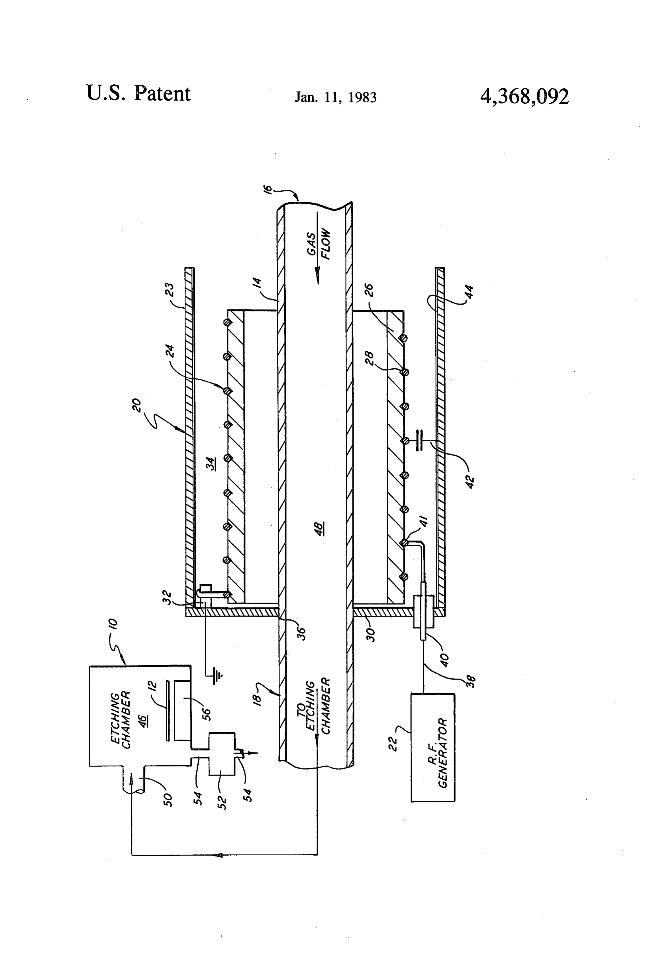
new and improved apparatus for etching semiconductor BRIEF DESCRIPTION OF THE DRAWING devices comprising, in combination; an etching cham ber containing the semiconductor device to be etched, The FIGURE is a side elevation, partially in section and an electrodeless etching plasma forming chamber and partially schematic, showing a preferred embodi having an inlet connected to a source of continuous ment of the present invention.
flowing etching gas and having an outlet connected to DETAILED DESCRIPTION OF A PREFERRED the etching chamber in fluid flow communication. A EMBODIMENT helical inductive resonator coupler is provided for cou pling a source of R.F. electrical power into said elec 65 In the embodiment of the invention illustrated in the trodeless plasma forming chamber for continuously drawing, apparatus for the downstream etching of a forming etching plasma from the etching gas flowing semiconductor device comprises, in combination, an therethrough. In one form of the invention the helical etching chamber 10 containing a semiconductor device
Page 4scan →
12 to be etched. An electrodeless tubular etching A trimming capacitor 42 may be provided between plasma forming chamber 4 is provided, which has an the wall of the cylinder 23 and the coil 24, as shown, to inlet indicated at 16 connected to a source of continu assist in providing a fine tune for adjusting the resonant ously flowing etching gas and has an outlet indicated 18 frequency of the coupler and plasma forming circuit, connected to the etching chamber 10 in fluid flow com when the plasma forming chamber is operating, to the munication. A helical inductive resonator coupler indi resonant frequency of the R.F. generator. This capaci cated at 20 is provided for coupling a source 22 of R.F. tor may be eliminated by adjusting the resonant fre electric power into the electrodeless tubular etching quency of the generator, or by building the coupler 20 : plasma forming chamber for continuously forming with a precision which makes additional trimming un etching plasma from the etching gas flowing there 10 necessary.
through. As indicated hereinbefore, the length of the wire of A suitable type of inductive resonant coupler is the coil 24 is nominally one quarter of the freespace shown in U.S. Pat. No. 3,873,884 issued Mar. 25, 1975, wavelength of the R.F. power to be supplied by the for example, the helical inductive resonant coupler 20 is R.F. generator 22. The coupler and plasma forming made up of a hollow cylinder or shield can 23 of an 15 chamber configuration of this invention thus provides a electrically conductive material and a helical coil 24 compact, quarter-wave, transmission line resonator wound on a ceramic or alumina tube coil form 26 with which can be proportioned to have extremely low a spiral groove 28. One end of the cylinder 23, the right losses.
hand end is open; its other end is closed by a base mem The coupler 20 has, due to the general configuration ber 30, which is also of electrically conductive material. 20 shown, a high electrical Q. This is enhanced by making The base member 30 is grounded at the R.F. connector the coupler of low loss materials and reducing losses by 40 by the shield of the coaxial cable 38, and is fixed in all practical means. In practice, the cylinder 23 and base the end of the cylinder so that the cylinder is electri member 30 are made of copper or brass and the interior cally connected to the base member and thus similarly of the cylinder is plated with a polished silver coating as connected to ground. 25 indicated at 44 in the drawing, and the wire of the coil One end of the coil 24, the left hand end as shown, is 24 is solid silver, copper wire or silver plated copper for grounded by being connected to the base member as at the purpose of maintaining high R.F. conductivity. the ground terminal 32; its other end is unconnected and Also, soldered taps are avoided, the taps preferably thus open circuited. Preferably, the length of the wire of being welded or silver soldered. coil 24 is made one quarter of the wavelength of the 30 When the power from the R.F. generator 22 is first R.F. electric power to be supplied by the R.F. genera applied to the coupler 20 and the etching plasma has not tor 22. The diameter of the coil 24 is less than the inside yet started to form in chamber 14, i.e., discharge has not diameter of the cylinder 23 so as to provide an annular yet started, the resistance and reactance reflected by the air space 34 between them. The coil and cylinder are discharge in the chamber 14 when the plasma forming thus in a capacitor relationship. In practice, the relative 35 process is in operation are absent. Because the plasma diameters of the cylinder and coil may, for example, be forming chamber is not extracting power and the cou approximately 4 inches and 2 inches, respectively, so pler has a very high electrical Q and the open circuited that the gap therebetween is about 15/16 inch. The end of the coil 24 is the location of a current node and cylinder is preferably made slightly longer than the coil hence a voltage maximum, the input R.F. voltage swing to provide a suitably long ground plane relative to the 40 is transformed to a very high voltage (e.g., about ten field of the last turn of the coil at its open-circuited end thousand of volts) at the open circuited end of the coil. to avoid unwanted fringe effects. In the embodiment This high voltage creates a potential through the gas in shown, the open end of the cylinder 23 extends beyond the plasma forming chamber 14 to the grounded base the amount necessary to avoid fringe effects. member 30 of the cylinder which ionizes the gas. The The electrodeless etching plasma chamber 14 is con 45 electrostatic energy thus coupled into the plasma form centrically mounted in the cylinder 23 as by means of ing chamber is enough to ionize the gas and start the the base 30, as indicated at 36. discharge.
R.F. electrical power is applied to the coil 24 from When the discharge starts, the Q of the coupler 20 the R.F. generator 22, for example, by means of a coax drops, the high voltage subsides and the plasma forming ial cable 38, which passes through a connector 40 50 chamber is thereafter maintained in operation by power mounted in the base member 30 to a tap 41 into the coil. in the turns of the coil 24. If the discharge should extin It is normally desired to have the plasma forming cham guish, voltage builds up in the open circuited end of the ber 14 and coupler 20 spaced some distance from the coil again, and discharge will then automatically reig R.F. generator 22 for flexibility of instrument design; in nite. When the plasma forming chamber is operating, this case, as illustrated, the R.F. generator 22 is shown 55 the voltage drop back as just described and the impe connected to the R.F. connector 40 through a coaxial dance of the circuit of the coupler 20 and the plasma cable 38. The R.F. generator is comparable to a conven forming chamber 14 then matches the impedance of the tional radio transmitter, which would be a suitable R.F. R.F. supply at the tap 41, thereby providing highly source. The R.F. generator 22 is operated from a con efficient operation of the plasma forming chamber. ventional source of electric power, not shown, and in 60 The interior 46 of the etching chamber 10 communi practice the R.F. generator is built to supply R.F. elec cates with the interior 48 of the tubular etching plasma trical power at 13.56 MHz at levels up to 300 to 400 forming chamber 14 via a conduit indicated at 50 in the watts and having an impedance of 50 ohms. drawing. The interior 46 of the etching chamber is The tap 41 into the coil 24 is located relative to the connected to a pump 52 via a port 54 for evacuating grounded end of the coil so that when the plasma form 65 gases and maintaining the pressure therein at a predeter ing chamber is operating the impedance of the coupler mined value suitable for etching. That is, in evacuating and plasma forming circuit matches the impedance of the gases from the etching chamber 10, the gases carry the R.F. generator at the tap 41. with them the products of etching. Within the chamber
Page 5scan →
10, this wafer 12 to be etched is disposed on a platform electrical coupling means for applying to the coil a 56, provided for the purposes. source of R.F. electrical power that is sufficient to in operation, when the source of etching gases is maintain a discharge in said plasma forming cham connected to the electrodeless etching plasma forming ber mounted within the coil, said coupling means chamber 14 and pump 52 is on, the etching gases flow applying power into the coil at a position near, but into the interior 48 of the chamber 14. When the R.F. spaced from, the grounded end thereof, said posi generator 22 is actuated, a plasma of the etching gas in tion being selected such that, when said plasma its excited state flows into the interior 46 of the etching forming chamber is in operation by the R.F. power chamber 10 where they attack and remove the desired 10 being applied to the coil, the impedance of said material from the wafer 12. When stripping photoresist plasma forming chamber and coupling means at from a wafer, the etching gas is composed of 1 part of said position substantially matches the impedance CF4 to 25 parts of O2. When silicon is etched 7 parts of of said R.F. power source, whereby when said CF4 to 2 parts of O2 are used for the etching gas. R.F. power is applied to the coil, and before a discharge is ignited in said plasma forming cham
Also, for both of these processes, the pressure in the 15 ber, a voltage maximum occurs at the end of the chambers 10 and 14 should be about 0.3 Torr (higher or coil remote from said grounded end and creates a lower pressures can be used) when gas is flowing and potential extending through the portion of said the discharge is on. Temperature of the wall of the tube plasma chamber between said end remote from the 14 is approximately 40 C. and the temperature in the grounded end and said base member for ionizing chamber 10 is approximately 23° C. the gas in said plasma forming chamber. Although a certain particular embodiment of the 2. Apparatus for the etching of semiconductor de invention is herein disclosed for purposes of explana vices according to claim wherein the end of said coil tion, various modifications thereof, after study of this remote from the grounded end thereof is open circuited. specification, will be apparent to those skilled in the art 3. Apparatus for the etching of semiconductor de to which the invention pertains. 25 vices according to claim 1 or claim 2 wherein the wire What is claimed and secured by Letters Patents is: of the coil is about one-quarter wave long relative to the 1. Apparatus for etching semiconductor devices com free space wavelength of the R.F. power intended to be prising, in combination: applied for operating the plasma forming chamber an etching chamber adapted to contain the semicon mounted therein.
ductor device to be etched; 30 4. Apparatus for the etching of semiconductor de an electrodeless etching plasma forming chamber vices according to claim 3, wherein the outside diame having an inlet connected to a source of continu ter of the coil is substantially one-half the inside diame ously flowable etching gas and having an outlet ter of the cylinder, the coil being of silver or copper connected to said etching chamber in fluid flow 35 wire and the interior of the cylinder being polished silver plating.
communication; 5. Apparatus for the etching of semiconductor de a helical inductive resonator coupler for coupling a vices according to claim 2, wherein the open end of the source of R.F. electrical power into said electrode cylinder extends beyond the open circuited end of the less plasma forming chamber for continuously coil at least sufficiently to avoid fringe effects. forming etching plasma from the etching gas flow 40 6. Apparatus for the etching of semiconductor de ing therethrough, said helical inductive resonator vices according to claim 1 or 2 wherein said base mem coupler comprising: ber extends across and substantially closes an end of the a grounded hollow cylinder of electrically conduc cylinder, the outside diameter of the coil and inside tive material with a grounded base member at one diameter of the cylinder being substantially 2 inches end thereof; 45 and 4 inches respectively, the wire of said coil being a helically coiled wire conductor concentrically silver or copper, and the interior walls of the cylinder mounted within the cylinder and spaced from the and base member being polished silver plating. inner walls thereof; 7. Apparatus for the etching of semiconductor de means for mounting said plasma forming chamber vices according to claim , further including pump substantially concentrically within the coil; 50 means connected to said etching chamber for evacuat the end of the coil toward said base member being ing said etching chamber at a predetermined rate. grounded, and sk
Provenance
- Collection
- Patents citing this work
- Pages
- 5
- Method
- pdftotext (the PDF's own text layer) + pdftoppm 300dpi page scans
- Patent office record
- patents.google.com →
- Source
- Google Patents citing-documents table
- Assignee
- The Perkin-Elmer Corporation
- Published
- 1983-01-11
- Transcribed from
- patentimages.storage.googleapis.com →