

patent · US4405406A
Plasma etching process and apparatus
20 September 1983
Text
Page 1scan →
United States Patent (19)
Casey et al.
(54) plasma etching process and
Apparatus
75 Inventors: Martin J. Casey, Mesa, Ariz.; John E. Sheppard, Bensalem, Pa.
73) Assignee: Sperry Corporation, New York, N.Y.
Related U.S. Application Data doned.
52 U.S. Cl. .................................... 156/643; 156/6
58) Field of Search ........... . . . . 156/643, 646, 653, 657,
Xxxxxxxxx
Xxxxxxxx
3,880,684 4/1975 Abe ................................ 252/79.1 X 3,984,301 10/1976 Matsuzaki et al. .. ... 204/192 E 4,233,109 11/1980 Nishizawa ........a swas a . . . . . 156/345
Other publications
Dry Process Technology (Reactive Ion Etching) by
Primary Examiner-William A. Powell
Attorney, Agent, or Firm-James R. Bell; Marshall M. Truex
A plasma etching process and apparatus wherein a gas plasma comprising dichlorofluoro-methane (CHCl2F) etches a film.
1 Claim, 6 Drawing Figures
Xxx xxxxx
Drawings
Page 2drawing sheetscan →
Page 3drawing sheetscan →
Page 4scan →
favorably solve problems such as those mentioned
PLASMA ETCHING PROCESS AND APPARATUS above. . .
This is a continuation of application Ser. No. 171,790, 5 SUMMARY filed July 24, 1980, now abandoned. The invention pertains to a process and apparatus for a high resolution, dry plasma etching process for fabri
BACKGROUND cating, semi-conductor devices. A plasma comprising This invention pertains to the fabrication of semi-con dichlorofluoro-methane (CHCl2F) etches portions of a ductor devices, and particularly to dry plasma etching O polysilicon film in a controlled reducing atmosphere. processes used in such fabrication. In one embodiment of the invention, a workpiece is Semi-conductor devices, such as semi-conductor in positioned on an electrode serving either as an anode or tegrated circuits, typically comprise a substrate, or base, a cathode and which is contained in a vacuum chamber. which has deposited thereon one or more film layers. piece In a second embodiment of the invention, the work Some such film layers have a dopant selectively dif 15 or is positionable in a vacuum chamber having one fused or otherwise loaded therein in accordance.with a more electrodes or an inductance coil external pattern indicative of the junctions to be formed in the thereto.
integrated circuit. The pattern may correspond, for cessAnand object of the invention is the provision of a pro apparatus wherein a polysilicon film is etched example, to portions of the film not temporarily cov in an efficient and economical manner without under ered by a photoresist or mask which shields the portions 20 cutting.
not to be doped. Before diffusing or loading the dopant into the film, however, select portions of the film layer gasAnplasma, advantage of the invention is the provision of a which efficiently and sharply etches por must first be removed, or etched, in accordance with tions of a polysilicon film without damaging a photore
One known technique for etching a film is plasma 25 sistAnother material covering unexposed portions of the film.
advantage of the invention is the provision etching. Plasma etching is the selective removal of ma of a gas plasma which etches polysilicon at a rate of at terial by reaction with chemically active gases createdleast 15 times faster than the rate at which it etches by a radio frequency (RF) power-induced glow dis silicon dioxide.
charge environment. In plasma etching, the RF voltage applied across the gas normally causes the gases to 30 sion of apparatusadvantage
Yet another of the invention is the provi for practicing the process of the inven disassociate and to form various free radicals which tion.
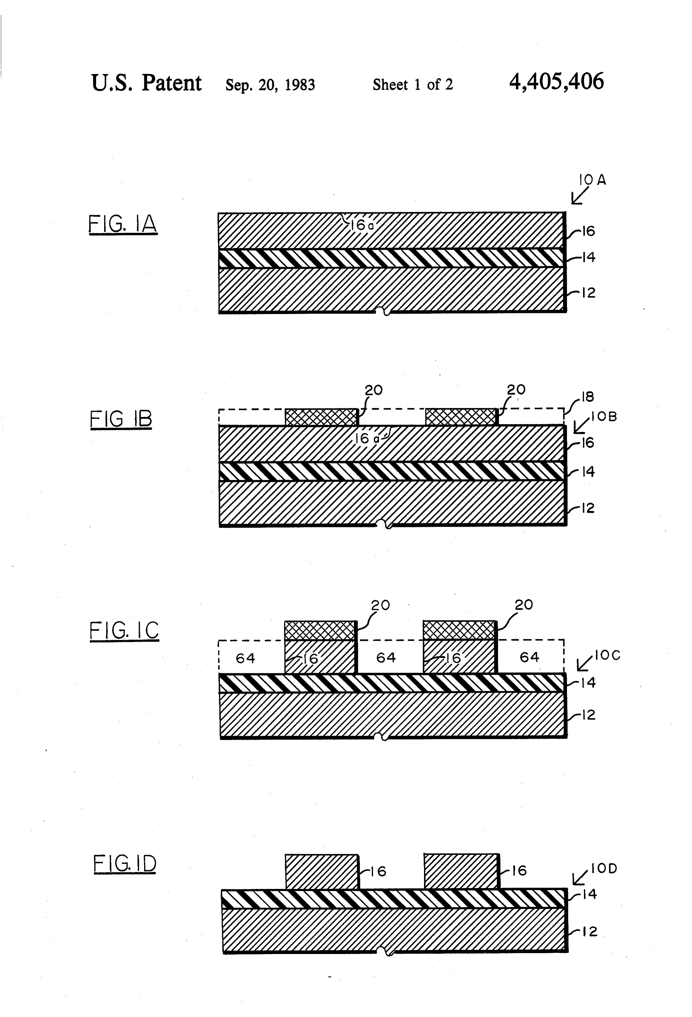
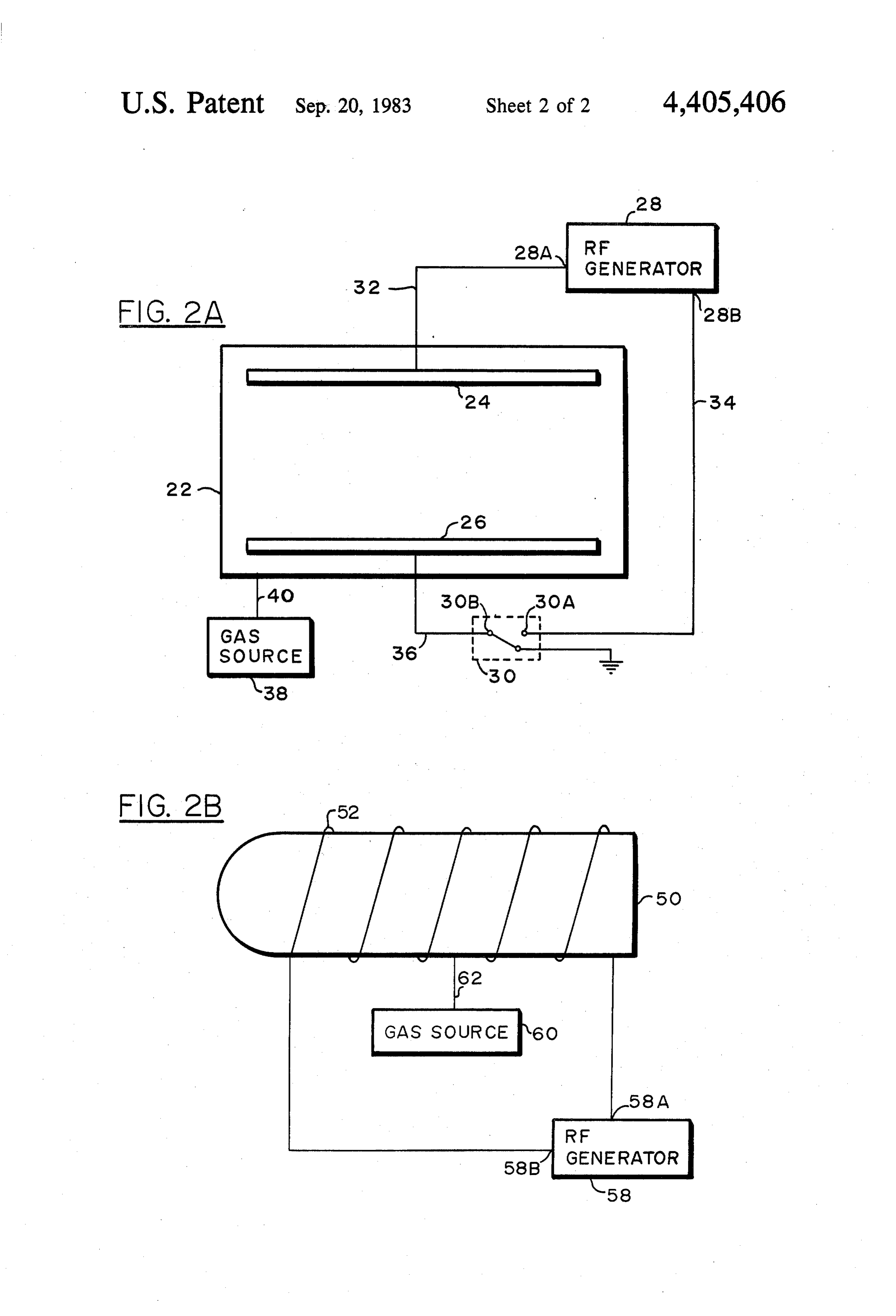
chemically interact to etch away the select areas of the film for subsequent doping. BRIEF DESCRIPTION OF THE DRAWINGS Apparatus used for plasma etching is of two basic The foregoing and other objects, features and advan types. In the first, one or more electrodes or an induc 35 tages of the invention will be apparent from the follow tance coil is external to a vacuum chamber into which a ing more particular description of the preferred embodi semi-conductor workpiece is inserted. In the second ments of the invention, as illustrated in the accompany type of apparatus, the workpiece is placed on a cathode ing drawings in which like reference characters refer to which, along with an anode, is internally contained in the same parts throughout different views. The draw the vacuum chamber. 40 ings are not necessarily to scale, emphasis instead being While plasma etching is generally thought to be a placed upon illustrating the principles of the invention. cleaner, more economical, and more desirable tech FIGS. 1A, 1B, 1C and 1D are cross-sectional views nique than the wet chemical etching techniques hereto illustrating semi-conductor workpieces undergoing var fore known, various factors (such as the composition of ious fabrication steps included in the process of the the film-to-be-etched and any neighboring films, as well 45 invention; and, as the composition of the gas employed in the process) FIGS. 2A and 2B are schematic view of apparatus determine whether the particular plasma etching pro according to two differing embodiments of the inven cess employed: overcomes various potential problems tion.
associated with the process. Such problems include, for DETAILED DESCRIPTION OF THE example, the fact that in some processes the etching rate 50 DRAWINGS of the exposed portions of the film-to-be-etched is not significantly greater than that of neighboring or under FIG. 1A illustrates a semi-conductor workpiece 10A lying films which are not to be etched. Likewise, in at a stage of fabrication preliminary to the etching pro some instances, the gas plasma has a deleterious effect cess of the invention. The workpiece 10A comprises a on the photoresist which serves to shield the portions of 55 substrate 12 (only a portion of which is depicted in the film which are not to be etched. FIGS. 1A through 1D) which has been placed in a Another important consideration in the plasma etch furnace or the like to produce a thin oxide film 14 ing process is the degree of accuracy or sharpness with thereon. In a preferred embodiment, the substrate 12 which the plasma etches only the selected portions of comprises silicon (Si) and the oxide film 14 comprises a the film. The plasma should not, while etching an ex 60 silicon dioxide (SiO2) layer approximating 700 ang posed portion of the film, undercut into a neighboring stroms (A) in thickness. A film-to-be-etched 16, prefer portion of the same film which is not to be etched. . . rably of polycrystalline silicon (polysilicon), and prefer Various semi-conductor devices currently available rably equal to or less than 5,000 A, has been deposited comprise, a polycrystalline silicon (polysilicon) film on the substrate 12 and oxide film 14 by a conventional deposited on a substrate. In many cases the substrate has 65 technique, such as chemical vapor deposition. an oxidized silicon coating onto which the polysilicon is Subsequent to the fabrication step depicted in FIG, deposited. However, the particular gases presently em 1A, a photosensitive material (not shown in FIG. 1A) is ployed to etch a film, such as a polysilicon film, do not applied to an upper surface 16a of the film-to-be-etched
Page 5scan →
16. The photosensitive material, such as a conventional it should be understood that various appropriate struc photoresist, is photolithographically or otherwise. pat tural features, such as a vacuum pump, matching net terned according to a junction pattern to be replicated work, flowmeter, and control valve may be incorpo in the underlying film 16. The photoresist is then pro rated into the embodiment of FIG. 2B although not cessed to remove select portions thereof and thereby necessarily illustrated as such. expose corresponding portions of the film-to-be-etched The embodiment of FIG. 2B may also be oriented so 16. The results of these fabrication steps are shown in that either first terminal 58A or second terminal 58B of FIG. 1B, wherein dashed lines 18 depict the photoresist the generator 58 is the neighboring terminal. Typical as originally applied and the numerals 20 indicate the power remaining photoresist portions which still cover por 10 FIG. 2Blevels for the operation of the embodiment of are 0.1 to 0.4 watts/cm2 at 13.5 MHz and pres tions of the film 16. sures of 150 to 400 milli-torr. A workpiece 10B similar to that illustrated in FIG. Activation of the switches 30 and 54 in the embodi 1B is then placed into apparatus resembling either the ments of FIGS. 2A and 2B close the respective electri embodiment illustrated in FIG. 2A or FIG. 2B. The embodiment of FIG. 2A comprises a vacuum chamber 15 cal circuits and thereby create a radio frequency power induced glow discharge environment in the respective 22 which may be constructed from various materials vacuum chambers 22 and 50. The RF voltage applied such as metal or glass, for example. A first electrode 24 and a second electrode 26 are positioned in parallel across the dichlorofluoro-methane gas supplied to the chambers causes the dichlorofluoro-methane to disasso fashion within the vacuum chamber 22.
The apparatus of FIG. 2A also comprises an electri 20 ciate and to form various free radicals which chemically cal circuit including a radio frequency (RF) generator interact to etch away the select areas of the film 16 28 and an electrical switch 30. The RF generator has a which are to be doped. FIG. 1C illustrates the appear first terminal 28A connected by a suitable wire 32 to the ance of a workpiece 10C upon completion of the etch first electrode 24. A second terminal 28B of the RF ing process as conducted in either the embodiment of generator 28 is connected by a wire 34 to terminal 30A 25 the apparatus illustrated in FIG. 2A or FIG. 2B, show of switch 30. Terminal 30B of switch 30 is connected by ing by dashed lines etched-away portions 64 of the film wire 36 to the second electrode 26. 16. The portions 64 are those select areas of the film 16 The apparatus of FIG. 2A further comprises a source which are to be subsequently doped.
38 of dichlorofluoro-methane (CHCl2F) gas. The As illustrated in FIG, 1C, the oxide film 14 on sub source 38 is in selective fluid communication with the 30 strate 12 is untouched by the etching process. Since it is vacuum chamber 22 by an appropriate fluid connector very difficult to deposit the film 16 onto the workpiece 40. 10 with a uniform thickness, it is likely that etching of It should be understood that the embodiment of FIG. some portions of the film may be completed before 2A may further incorporate other structural features other portions. In such cases the oxide film 14 becomes which are not necessarily discussed herein. For exam 35 and remains exposed to the plasma while the etching ple, a flowmeter and/or control valve may be posi continues for other portions of the film. Thus, it is tioned along the fluid connector 40 intermediate the highly desirable that the etching rate of the film 16 be source 38 and the chamber 22. Likewise, an exhaust significantly greater than the etching rate of the oxide port may be provided for selectively allowing gas to film 14. In this regard, when using dichlorofluoro escape from the chamber 22. Other known features not 40 methane in accordance with this invention, the etching specifically illustrated herein also include a matching rate of polysilicon film (such as film 16) is greater than network (operative in conjunction with the RF genera 15 times the etching rate of a film of silicon dioxide tor 28), electrode supports, and a vacuum pump.
In operating the embodiment of the apparatus illus (such The as film 14).
etched-workpiece 10C of FIG. 1C also illustrates trated in FIG. 2A, the RF generator 28 may be con the sharpness with which the plasma etches only the nected so that terminal 28A thereof corresponds either select portions of the film 16. In this regard, the plasma to a positive terminal or to a negative terminal, meaning does not undercut from the region 64 into the portions that the first electrode 24 can function as either an anode or a cathode. For example, when terminal 28A of of the film which are not to be etched. Moreover, the RF generator 28 is negative and terminal 28B is posi 50 coveringdoes plasma not damage the photoresist material 20 the unexposed portions of the etched film 16.
tive, the first electrode 24 functions as a cathode. Thus, Upon completion of the etching process as described depending on the manner in which the RF generator 28 above, is connected, either electrode 24 or 26 may function as removethe workpiece 10C of FIG. 1C is processed to the remaining photoresist portions 20. Such an anode or cathode regardless of the location of the workpiece 10 within the chamber 22. In either mode, 55 processing may be conducted by a number of standard typical power levels are 0.20 to 0.70 watts/cm2 at 13.5 techniques, resulting in a workpiece 10D appearing in MHz and chamber pressures are between 150 and 400 FIG. 1D.
milli-torr. While the invention has been particularly shown and In the embodiment of the apparatus illustrated in described with reference to the preferred embodiments FIG. 2B, a vacuum chamber 50 has an inductance coil 60 thereof, it will be: understood by those skilled in the art 52 wrapped therearound. The inductance coil 52 is that various alterations in form and detail may be made powered by an radio frequency generator 58. One side therein without departing from the spirit and scope of of the coil 52 is connected to terminal 58A, and the the invention. .
other side of the coil 52 is connected to terminal 58B of The embodiments of the invention in which an exclu the radio frequency generator 58. 65 sive property or privilege is claimed are defined as As in the embodiment of FIG. 2A, a source of di follows:
chlorofluoro-methane gas 60 is in communication with 1. A method of selectively etching a film comprising the vacuum chamber 50 by a fluid connector 62. Again the steps of:
Page 6scan →
depositing a polycrystalline silicon film on an underlying substrate comprising silicon dioxide thereby
1nserting Sald polycrystalline Slicon film on said underlying substrate into a vacuum chamber; 5 supplying dichlorofluoro-methane gas to said vacuum chamber;
applying a radio frequency voltage across said dichlorofluoro-methane gas supplied to said chamber, thereby causing said gas to disassociate and form radicals which chemically interact to etch select areas of said film, said film being etched substantially without lateral etching and said select areas of said film being etched at a rate essentially 15 times greater than the etching rate of silicon dioxide comprising said substrate.
Provenance
- Collection
- Patents citing this work
- Pages
- 6
- Method
- pdftotext (the PDF's own text layer) + pdftoppm 300dpi page scans
- Patent office record
- patents.google.com →
- Source
- Google Patents citing-documents table
- Assignee
- Sperry Corporation
- Published
- 1983-09-20
- Transcribed from
- patentimages.storage.googleapis.com →