

patent · US4450031A
Ion shower apparatus
22 May 1984
Text
Page 1bibliographic recordscan →
United States Patent (19) 4,450,031 Ono et al. (45) May 22, 1984 (54) ION SHOWER APPARATUS Dr. L. D. Bollinger, pp. 66-70, Nov. 1977/Solid State (75) Inventors: Toshiro Ono; Seitaro Matsuo, both of Technology.
Isehara, Japan Ion Beam Divergence Characteristics of Two-Grid Assignee: Nippon Telegraph & Telephone. Accelerator Systems, G. Aston et al., pp. 516-524, Public Corporation, Tokyo, Japan AIAA Journal, vol. 16, No. 5, May 1978. 21 Appl. No.: 530,424 Primary Examiner-William A. Powell Attorney, Agent, or Firm-Cushman, Darby & Cushman
(30) Foreign Application Priority Data (57) ABSTRACT Sep. 10, 1982 JP Japan ................................ 57-156842 An ion shower apparatus comprising a plasma forma Oct. 4, 1982 JP Japan ................................ 57-173270 tion chamber in which plasma is produced so as to produce ions, a single ion extraction grid disposed in Int. Cl. ........................ C23F1/02; CO3C 15/00; one portion of the plasma formation chamber and for B44C 1/22; H01L 21/306 extracting the ions from the plasma formation chamber 52 U.S.C. .................................... 156/345; 118/728; so as to form an ion beam in the form of shower, a 118/50.1; 118/620; 156/643; 156/646; 204/298 specimen chamber in which the surface of a specimen Field of Search ....................... 156/345, 643, 646; subjected to etching or deposition or a target subjected 204/192 R, 192 C, 192 EC, 192 S, 192 E, 298; to sputtering is irradiated with the ion beam in the form 427/38, 39; 118/715, 728, 50.1, 50, 620 of shower, and a shield grid disposed in the vicinity of References Cited the ion extraction grid in the plasma formation chamber
sheath produced over the ion extraction grid, in a man 4,233,109 11/1980 Nishizawa ....................... 156/345 X ner that the shield grid permits the passage of the 4,243,506 1/1981 Ikeda et al. ..................... 156/345 X plasma therethrough and prevents the electric field 4,259,145 3/1981 Harper ................................ 156/643 produced by the ion extraction grid substantially from OTHER PUBLICATIONS extending to the remaining region of the plasma forma Low Energy Ion Beam Etching, J. M. E. Harper et al., tion chamber. The ion extraction grid is not damaged. pp. 1077-1083, J. Electrochem. Soc.:Solid-State Sci An ion beam with a high current is obtained stably, ence and Technology, vol. 128, No. 5, May 1981.
Ion Milling for Semiconductor Production Processes, 9 Claims, 18 Drawing Figures
Drawings
Page 2drawing sheetscan →
Page 3drawing sheetscan →
Page 4drawing sheetscan →
Page 5drawing sheetscan →
Page 6drawing sheetscan →
Page 7drawing sheetscan →
Page 8drawing sheetscan →
Page 9drawing sheetscan →
Page 10drawing sheetscan →
Page 11drawing sheetscan →
Page 12drawing sheetscan →
Page 13drawing sheetscan →
Page 14drawing sheetscan →
Page 15drawing sheetscan →
Page 16scan →
tics of Two-Grid Accelerator Systems', by G. Aston et
ION SHOWER APPARATUS al., AIAAJOURNAL, Vol. 16, No. 5, pp. 516–524. FIG. 2 shows an ion source of a prior artion shower
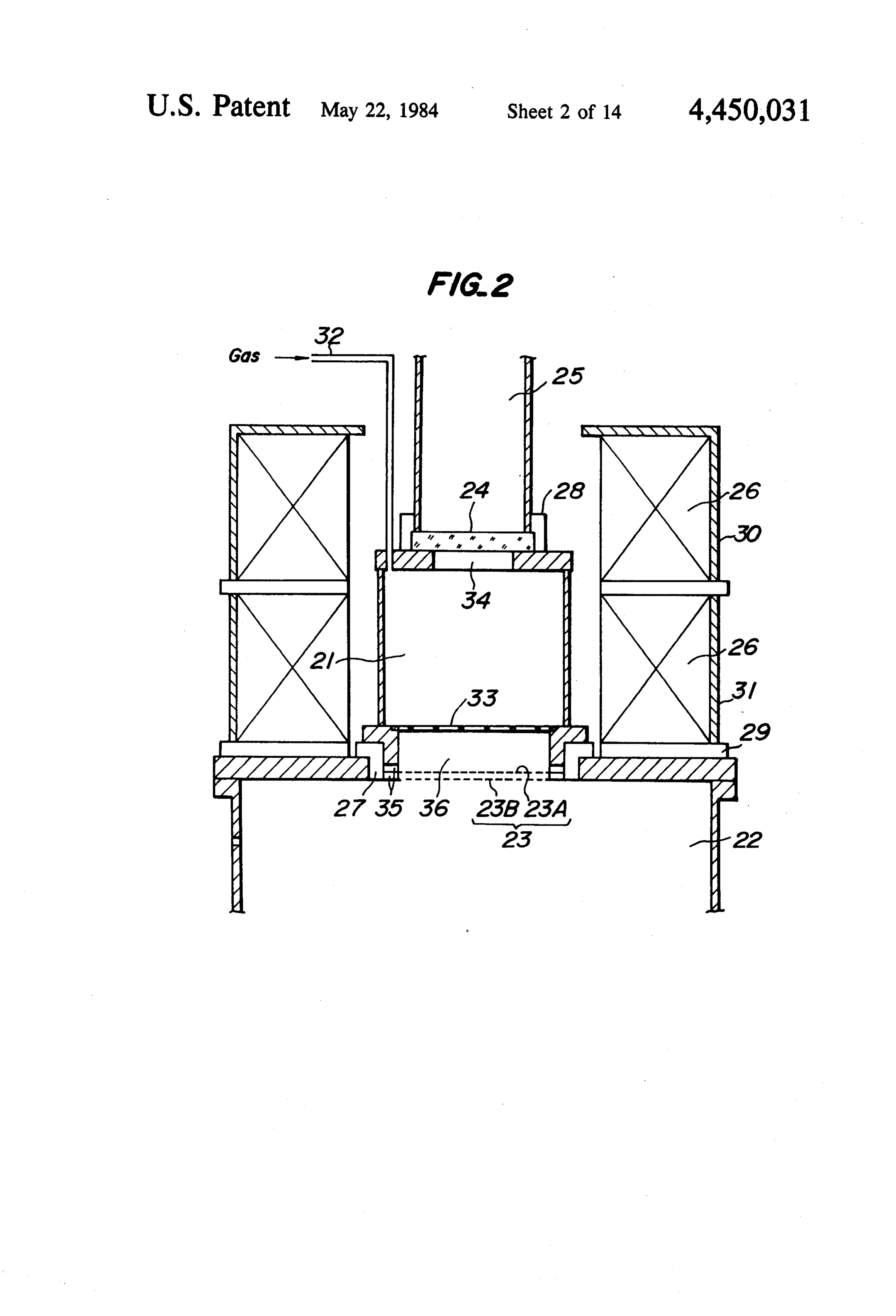
BACKGROUND OF THE INVENTION apparatus of the type in which plasma is produced by 1. Field of the Invention electron cyclotron resonance excited by microwave. The present invention relates to an ion shower appa The construction of the apparatus is disclosed in detail ratus for use in the process of etching fine patterns in the in Japanese Patent Application No. 61,409/1981. In FIG. 2, reference numeral 21 denotes a plasma forma manufacture of semiconductor devices, for use in the tion chamber; 22, a specimen chamber; 23, an ion ex process of sputtering a target by an ion current, for use 10 in the process of ion beam deposition on a specimen traction trode or grid assembly having an upper floating elec grid 23A and a lower ion extraction grid 23B;
surface of the like. 24, a microwave introducing window made of fused 2. Description of the Prior Art quartz; 25, a rectangular waveguide;26, a magnetic coil; The ion shower apparatus of the type described above comprises, in general, a plasma formation cham 15 27, 28 and 29, insulators; 30 and 31, magnetic shield ber for producing a plasma producing ions; ion extrac microwavewith members a high permeability; 32, a gas inlet; 33, a reflector; 34, a microwave coupling win tion grids so disposed as to partially define the plasma dow;35, an insulating spacer; and 36, a plasma transport formation chamber thereby extracting the ions from the chamber.
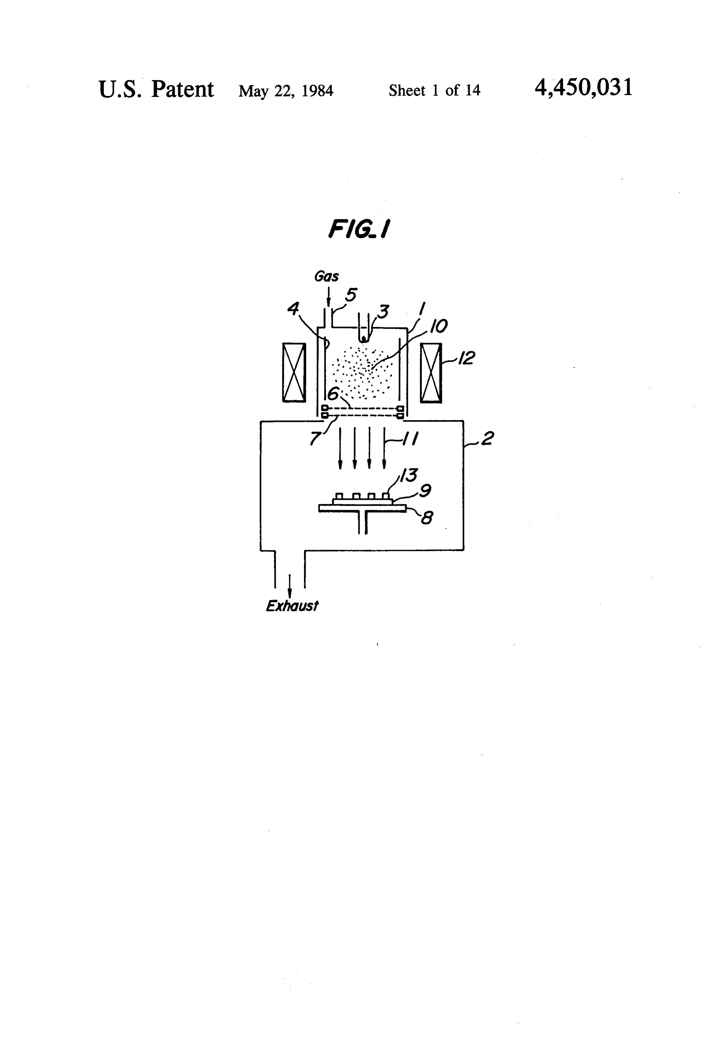
plasma formation chamber so as to produce anion beam When the ion source shown in FIG. 2 is operated, in the form of a shower (to be referred to as "a shower 20 first, a gas is introduced through the gas inlet 32 to the like ion beam" in this specification) and a specimen plasma formation chamber 21, while the microwave is chamber in which the surface of a specimen is irradiated introduced into the plasma formation chamber 21 with the shower-like ion beam. Such an ion shower through the rectangular waveguide 25, the microwave apparatus is widely used in the manufacture of semicon introducing window 23 and the microwave coupling ductor devices by using an ion etching or reactive ion 25 window 34. At the same time, the magnet coil 27 pro etching method, an ion beam sputtering method or an duces a magnetic field which satisfies a condition of ion beam deposition method. electron cyclotron resonance at least at one portion in FIG. 1 shows a Kaufman type ion shower apparatus the plasma formation chamber 21, so that plasma is which has been widely used. Such an apparatus is dis produced in the plasma formation chamber 21. In order closed in detail, for example, in "Ion Milling for Semi 30 that the microwave power is efficiently absorbed by the conductor Production Processes', L. D. Bollinger; plasma, the plasma formation chamber 21 is in the form Solid State Technology, Nov., pp. 66-70 (1977). In of a cavity resonator in which the microwave reflector FIG. 1, reference numeral 1 designates a plasma forma 33 is disposed, and the size and shape of the microwave tion chamber; 2, a specimen chamber; 3, a thermionic 35 reflector 33 is so selected that the microwave is re flected back by the microwave reflector 33 but the cathode; 4, an anode; 5, an etching gas inlet; 6 and 7, an plasma upper and a lower ion extraction electrode or grid;8, a the can freely pass through the reflector 33 toward specimen or substrate table;9, an object to be subjected plasma transport chamber. - to etching, deposition or sputterring, for example, a In order to extract the shower-like ion beam 11 from specimen or substrate; 10, plasma; 11, a shower-like ion 40 the plasma formation chamber 21 and the plasma trans port chamber 36 toward the specimen chamber 22, a beam; 12, a solenoid magnet; and 13, a mask.
In operation, an etching gas is introduced through the positive chamber potential is applied to the plasma formation 21 and the lower ion extraction grid 23B of the inlet 6 into the plasma formation chamber 1 and is ion ion extraction grid assembly 23 is grounded, while the ized by electrones accelerated from the thermionic upper ion extraction cathode 3 to the anode 4. The solenoid magnet 12 is 45 The insulating spacer grid 35 is 23A is electrically floated.
provided so that the upper used to increase an ionization efficiency. ion extraction grid 23A is electrically floated, and the Each of the ion extraction electrodes or grids 6 and 7 insulators 27 and 28 are provided in order has a plurality of apertures having a diameter of 2-3 mm potential to the plasma formation chamberto 21. apply a The and a high potential (for instance, 1000 V) is applied to upper ion extraction electrode 23A is floated, so that the plasma formation chamber 1 and to the upper elec SO negative potential is induced in a self-regulation mannera trode 6, while the lower electrode 7 is grounded. The depending upon the electron energy in the plasma. As a boundary of the plasma sheath is defined in the vicinity result, the number of incident electrons is considerably of the upper ion extraction grid 6 by the grid 6. The reduced, so that the upper and lower ion extraction ionized etching gas in the plasma 10 flows into the grids 23A and 23B are prevented from being heated and sheath boundary and is then accelerated by the electric 55 at the same time an abnormal discharge is suppressed. field in the plasma sheath, so that the ionized etching The magnetic shield member 31 with a high permeabil gas is extracted to the specimen chamber 2. As a result, ity covers the top and the outer periphery of the magnet in case that the shower-like ion beam 11 is used for the coil 27 so that a diverging magnetic field which is grad purpose of etching, the shower-like ion beam 11 im ually weakened toward the lower ion extraction grid pinges against the specimen or substrate 9 on the table 8, 23B is produced within the plasma formation chamber so that the surface of the specimen or substrate 9 which 21, whereby an ion extraction efficiency can be im is not covered by the mask 13 is physically or physio proved.
chemically etched. Further, the mask 13 is to be se According to Child's law, the relationship between lected from materials which do not react with the show an ion current density (J) of the ion current extracted er-like ion beam 11. 65 from the plasma formation chamber 21 to the specimen The dimensions of the two ion extraction grids 6 and chamber 22 and a voltage (V) applied between the 7 and the ion beam convergence at these grids are dis plasma formation chamber 21 and the ion extraction cussed in detail in "Ion Beam Divergence Characteris grid assembly 23 may be approximated as follows:
Page 17scan →
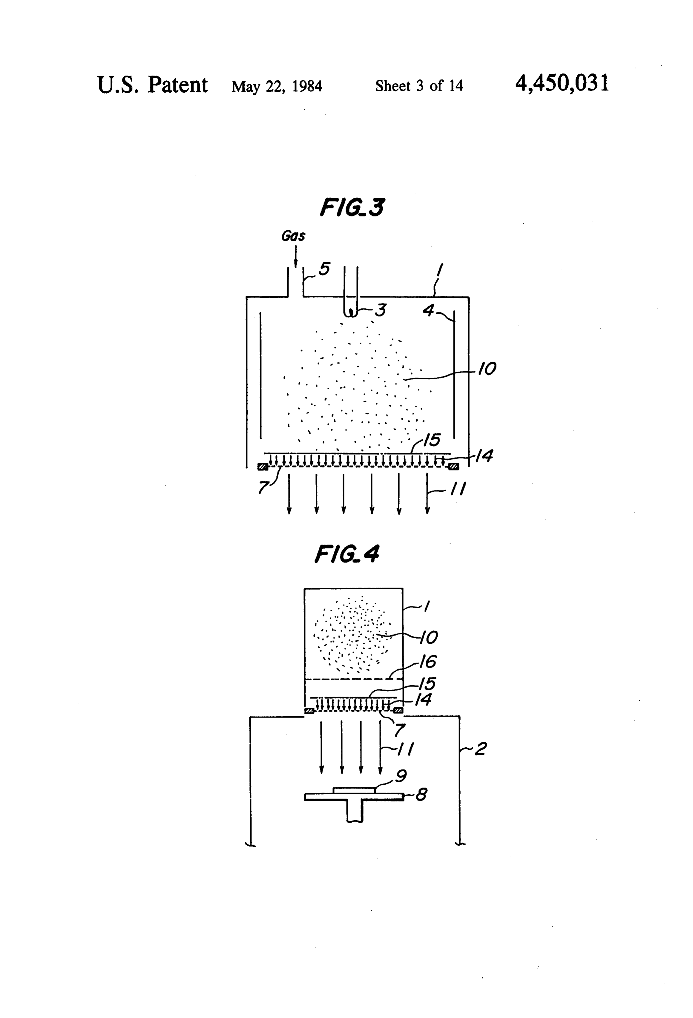
upper ion extraction grid 6 as shown in FIG. 1 is dis posed and the thickness of the plasma sheath 14 corre sponds to the distance 1 between the upper and lower where 1 is a distance between the ion extraction grids 6 ion extraction grids 6 and 7 as shown in FIG. 1. That is, and 7 or 23A and 23B. In the case of the ion shower the plasma sheath 14 acts as an imaginary upper ion apparatus of the type as shown in FIG. 1 or 2, the diam extraction grid. The thickness of the plasmasheath 14 is eter of the ion extraction grids 6 and 7 or 23A and 23B dependent on the voltage applied to the ion extraction is equal to or greater than that of the shower-like ion grid 7. For instance, when the applied voltage is 100 V, beam. The diameter is, in general, from 4 to 10 inches. the thickness of the plasma sheath 14 is in the order of In order that a uniform distance or gap may be main 10 0.1-0.2 mm. Therefore, as Child's law indicates, there tained between the two ion extraction grids having such exists an advantage that a high current density can be a large diameter as described above, the distance be tween the two grids is maintained to be 1 mm through obtained even at a low potential. 3 mm because thermal deformations must be taken into However, in the ion shower apparatus shown in FIG. consideration. Therefore, it follows that in order to 15 3, when a potential is applied to the ion extraction grid obtain the current density J which can attain a practical 7, the electric field thus produced is extended into the etching rate, a potential applied between the two ion whole plasma formation chamber 1 so that the dis extraction grids must be increased. charge electric field established between the thermionic For instance, in case that the ion shower apparatus as cathode 3 and the anode 4 for producing the plasma is shown in FIG. 2 is used for etching, when carbon fluo 20 considerably disturbed. As a result, abnormal dis ride gas (such as CF6, CFs) is introduced through the charges such as spark discharge tends to occur very inlet 32 into the ion shower apparatus so as to etch an frequently, and accordingly plasma cannot be sustained SiO2 film and when the voltage applied between the in a stable manner. Furthermore, according to Pas plasma formation chamber 21 and the grid 23B is 1000 chen's law, a spark-over occurs between the ion extrac V, a high etching rate of SiO2 film is obtained and a 25 tion grid 7 and particular a portion of the wall of the relatively high ratio of the etching rate of SiO2 film to plasma formation chamber 1, so that a stable ion beam an etching rate of Si is obtained. But, if the voltage cannot be produced when a high potential higher than applied between the plasma formation chamber 21 and 100-200 V is applied to the ion extraction grid 7. There the grid 23B is less than 500 V, the etching rate of a fore, as compared with the ion shower device with a SiO2 film and the ratio of the etching rate of a SiO2 film two-grid system as shown in FIG. 1, a practical etching to the etching rate of other material are low, which are rate, a good etching rate ratio of the etching rate to an not satisfactory in practice.
If the voltage applied between the two grids is in etching rate of other material, and an ion current suit able for ion beam sputtering cannot be attained, even creased for extracting ions for etching, a satisfactory though etching rate and a satisfactory etching rate ratio can be 35 tial less the than current density can be increased at a poten obtained, but abnormal discharge tends to occur be In addition, in order to produce a shower-like ion tween the grids. As a result, ions extracted by a high beam with a high degree of directivity, the diameter of potential damages crystal structures on the surface being etched so that the functions of the semiconductor the apertures of the ion extraction grid 7 is made sub devices are degraded. Thus, the ion shower apparatus 40 stantially equal to the thickness (0.1-0.2 mm) of the with a two grid system has a disadvantage in that its plasma sheath. Consequently, the ion extraction grid 7 application range is limited. There are also other disad must be machined or fabricated with a high degree of vantages in that a pertinent ion current cannot be ex accuracy, so that it is difficult to use the ion extraction tracted in case of ion beam sputtering by introducing an grid 7 in practice. Furthermore, the size of the rim Ar gas to the ion shower apparatus and in that it is 45 forming the ion extraction grid 7 must be substantially difficult to determine a low voltage which is preferable equal in dimension to or less than the fine apertures to an ion beam deposition process. In addition, there is thereof, so that the ion extraction grid 7 is easily sub a disadvantage in that there is involved a difficult work jected to thermal damage. Consequently, there is a dis of disposing and securing two grids in such a way that advantage in that a high current cannot be extracted. their apertures are correctly aligned or registered with each other. Moreover, it is difficult to obtain a uniform SUMMARY OF THE INVENTION ion shower with a large diameter. With the above in view, the present invention was FIG. 3 schematically shows an ion source of an ion made to overcome the above and other problems en shower apparatus of the type in which only one ion countered in prior art ion shower apparatuses. extraction grid is used. That is, the upper grid of the ion 55 It is, therefore, one of the objects of the present in shower apparatus as shown in FIG. 2 is eliminated. vention to provide an ion shower apparatus which can Such an ion shower apparatus is disclosed in detail in prevent damage to an ion extraction grid, whose opera “Low Energy Ion Beam Etching', by J. M. E. Harper et al.; J. Electrochem. Soc., Vol. 128, No. 5, pp. tion is not limited by a voltage applied to the ion extrac 1077-1083 (1981). In FIG. 3, the same reference numer high gridtion and which can obtain a stable ion beam with a current.
als as in FIG. 1 are used to designate the corresponding It is another object of the present invention to pro parts of the ion shower apparatus as shown in FIG. 1 vide an ion shower apparatus which can etch various are used to designate similar parts. It is seen in FIG. 3 that the upper ion extraction electrode 6 is eliminated. materials damage of semiconductor devices without causing any to them with a satisfactory etching rate and a
Reference numeral 14 designates a plasma sheath and 15, a sheath surface. In this apparatus, a plasma sheath is 65 satisfactory etching selectivity. produced in a self-regulation manner and an ion beam is It is a further object of the present invention to pro produced by the electric field in the plasma sheath. The vide an ion shower apparatus which can obtain stably sheath surface 15 is formed at the position at which the an ion current suitable for ion beam sputtering.
Page 18scan →
It is still a further object of the present invention to shower apparatus in accordance with the present inven provide an ion shower apparatus which is widely appli tion;
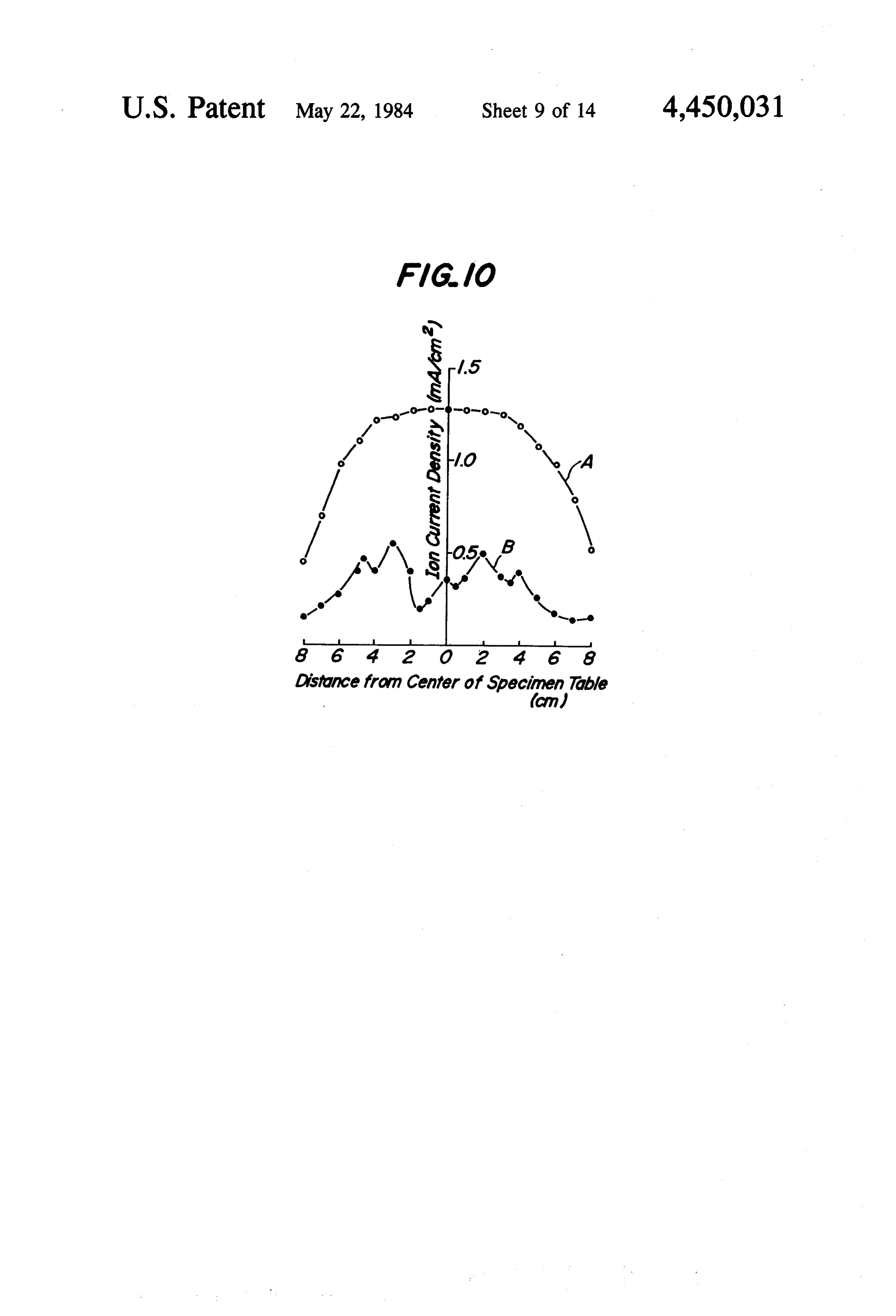
cable to ion beam deposition in which a relatively low FIG. 10 illustrates characteristic curves which in turn voltage is used as well as ion beam sputtering, ion etch show the uniformity of an ion shower produced in an ing and reactive ion etching in which a relatively high ion shower apparatus in accordance with the present voltage is used. invention;
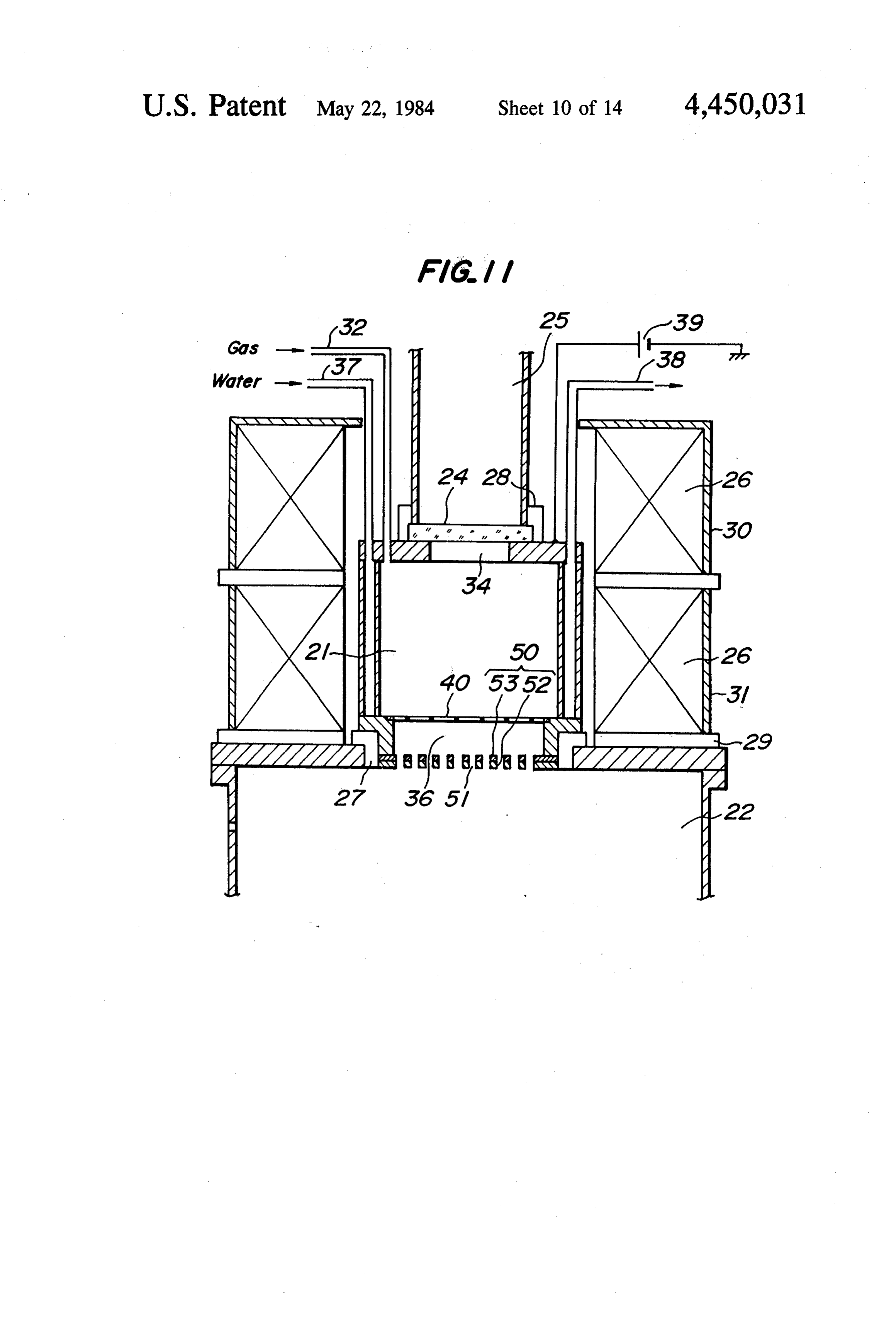
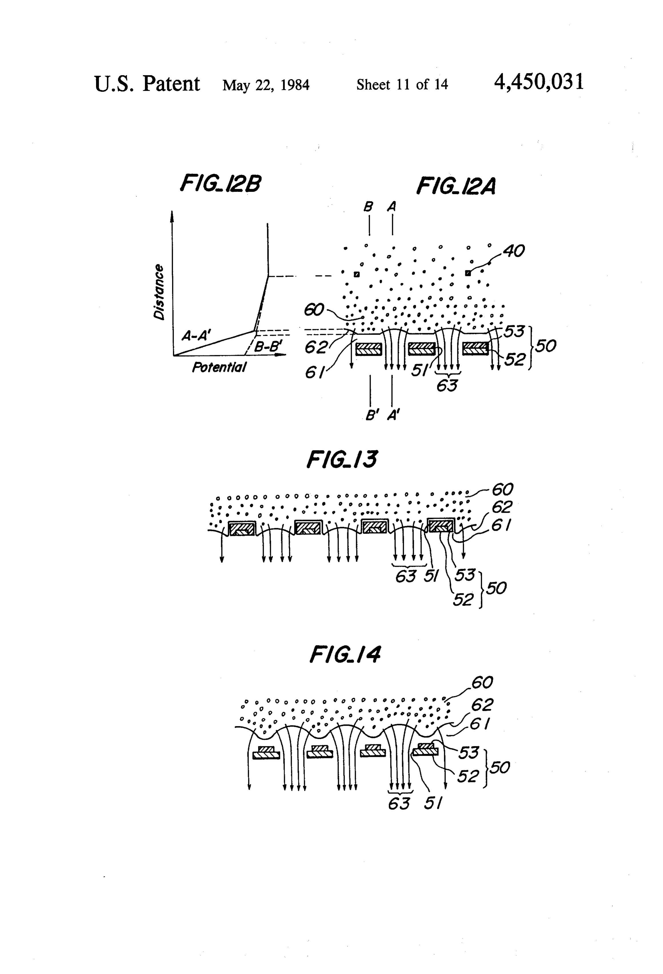
To the above and other ends, the present invention FIG. 11 is a sectional view schematically showing a provides an ion shower apparatus comprising a plasma third embodiment of the present invention; formation chamber in which a plasma is produced so as 10 FIGS. 12A, 13 and 14 are fragmentary sectional to produce ions; a single ion extraction grid disposed in views, respectively, on enlarged scale, of three exam one portion of the plasma formation chamber and for ples of an ion extraction grid of the ion shower appara extracting the ions from the plasma formation chamber tusFIG. shown in FIG. 11;
12B illustrates a potential distribution corre so as to form an ion beam in the form of shower; a specimen chamber in which the surface of a specimen 15 sponding to the ion extraction grid as shown in FIG. subjected to etching or deposition or a target subject to 12A;
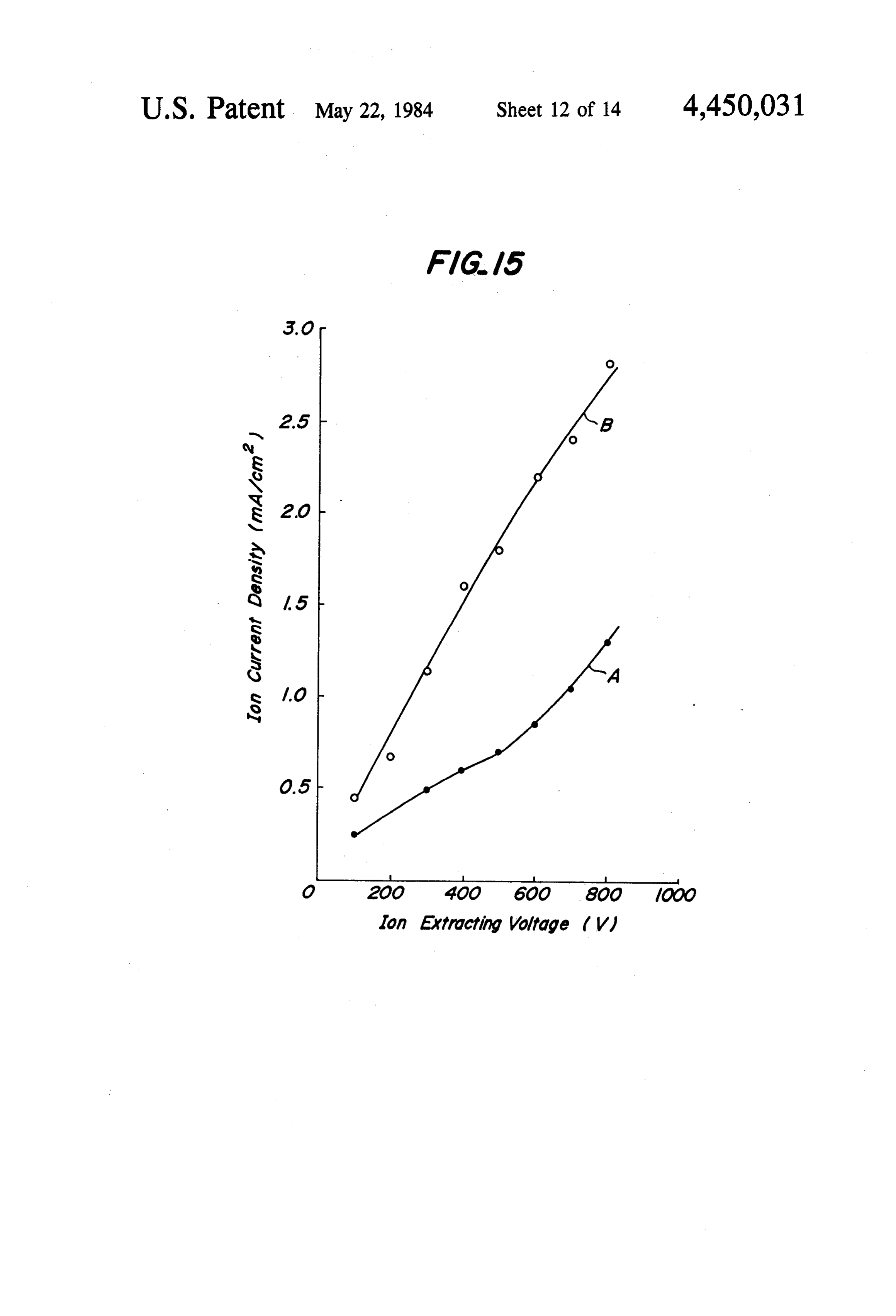
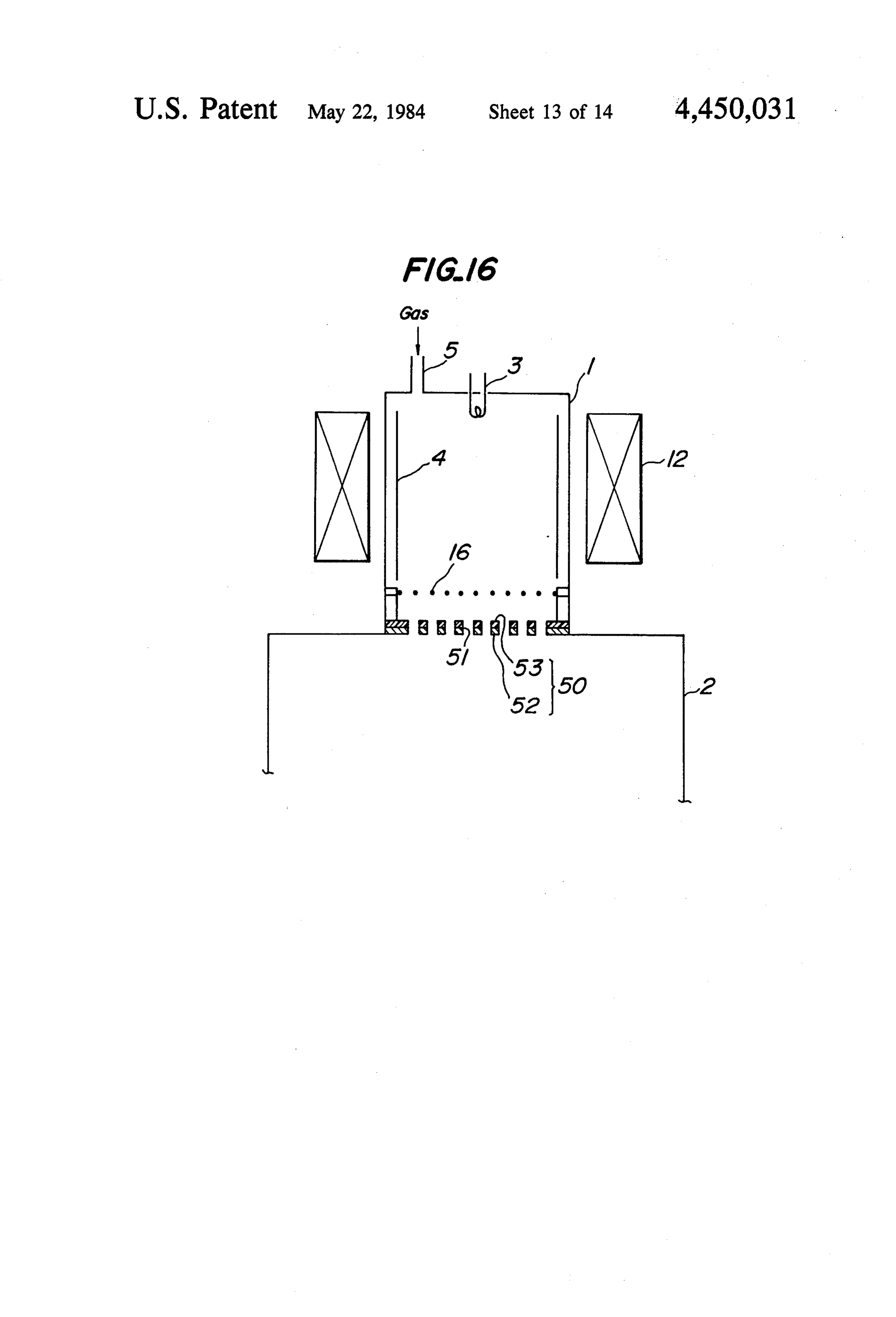
FIG. 15 illustrates a relationship between an ion ex sputtering is irradiated with the ion beam in the form of traction voltage and an ion current density of the ion shower; and a shield grid disposed in the vicinity of the shower apparatus ion extraction grid in the plasma formation chamber and shown in FIG. 11; spaced apart from the thickness of the plasma sheath 20 embodiment of the present diagram FIG. 16 is a schematic invention;
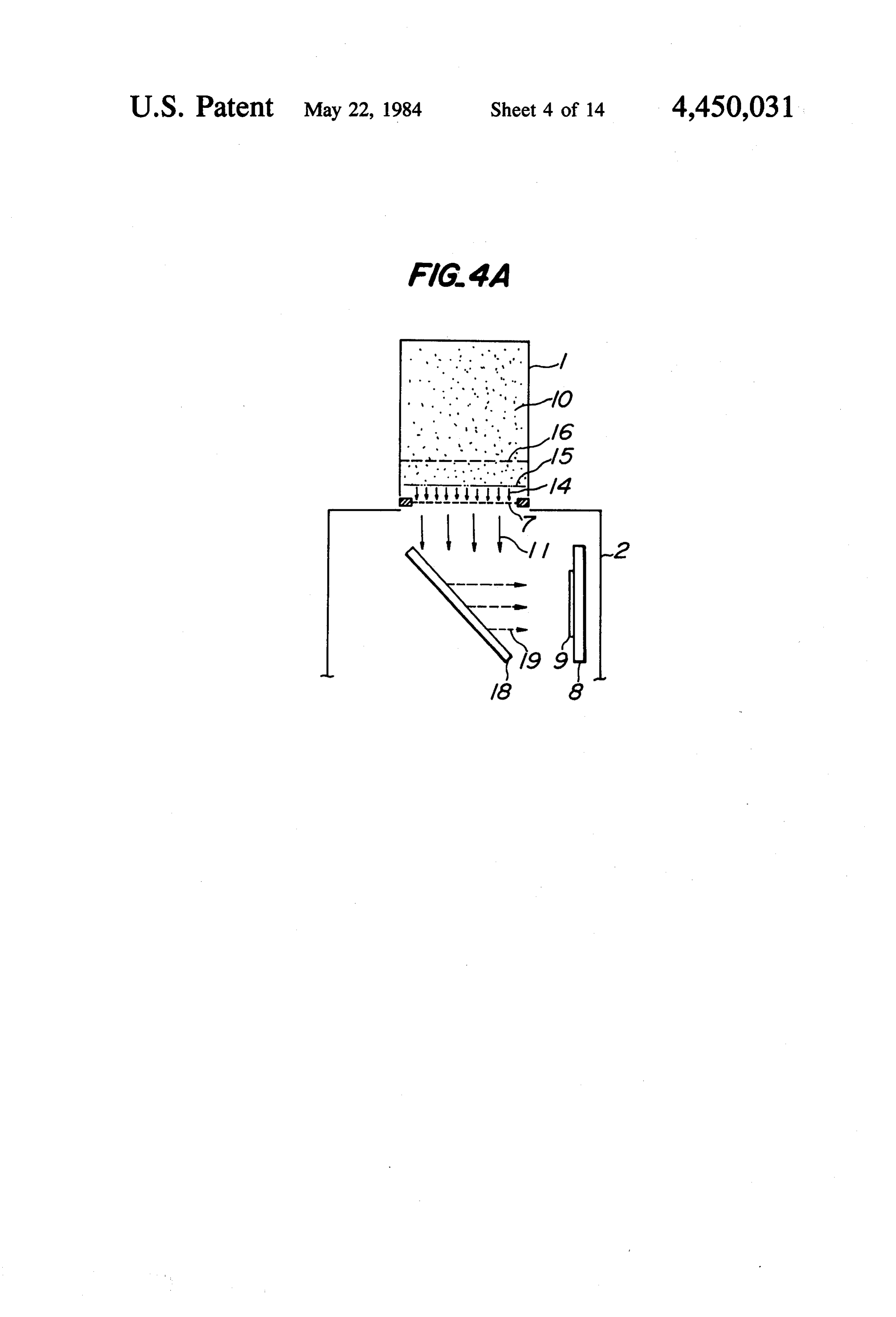
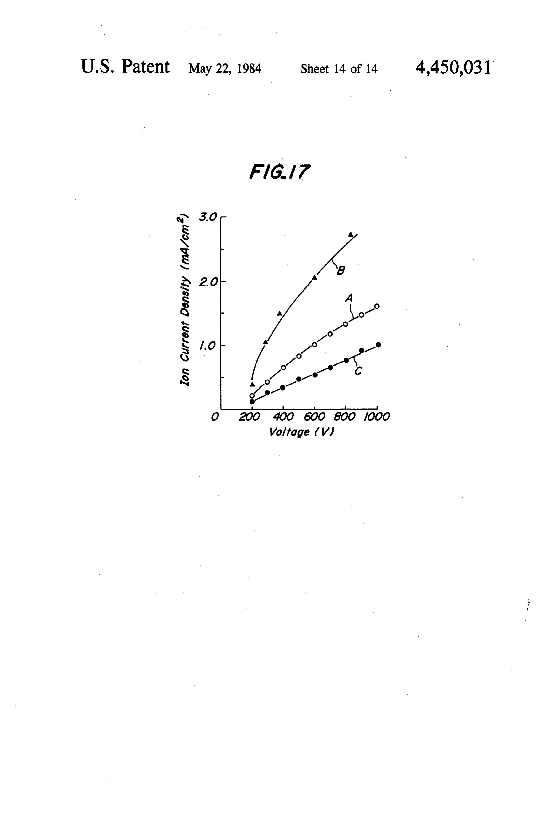
showing a fourth and produced over the ion extraction grid. The shield grid FIG. 17 illustrates a relationship between the applied permits the passage of the plasma therethrough and at voltage and the ion current density. the same time prevents the electric field produced by the ion extraction grid substantially from extending to DETAILED DESCRIPTION OF PREFERRED the remaining region orportion of the plasma formation 25 EMBODMENTS chamber. Same reference numerals are used to designate similar The above-described plasma can be produced in re parts throughout the figures. w sponse to the discharge caused by means of athermionic FIG. 4 shows a fundamental arrangement of an ion cathode or electron cyclotron resonance caused by shower apparatus in accordance with the present inven microwave. 30 tion. Reference numeral 1 denotes a plasma formation It is preferable that the ion extraction grid is made of chamber; 2, a specimen chamber; 7, a single ion extrac silicon or carbon. tion electrode; 8, a substrate table; 9, an object to be It is also preferable that an insulating member like an subjected to etching, deposition or sputtering, for exam insulating film is formed over the surface of the ion ple, a substrate or specimen; 10, plasma; 11, an ion beam extraction grid which is in contact with plasma. 35 in the form of a shower; 14, a plasma sheath; and 15, a BRIEF DESCRIPTION OF THE DRAWINGS sheath surface. According to the present invention, a shield electrode 16 is disposed in the vicinity of the
FIG. 1 is a schematic diagram showing a first exam extraction electrode 7 and is spaced apart from the ple of a prior artion shower apparatus for etching with thickness of the plasma sheath 14 formed above the ion a two-grid system; extraction electrode 7, so that the plasma 10 passes FIG. 2 is a sectional view schematically showing through the shield electrode 16 and at the same time the second example of a prior artion shower apparatus with electric field produced by the ion extraction electrode 7 a two-grid system; does not affect the remaining region of the plasma for FIG. 3 is a schematic diagram showing a third exam mation chamber 1. The potential applied to the shield ple of a prior artion shower apparatus with a single ion 45 electrode 16 is equal to the potential at the plasma for extraction grid; mation chamber 1.
FIG. 4 is a schematic diagram showing a fundamental Further, the above-described arrangement is for an arrangement of an ion shower apparatus in accordance ion shower apparatus for ion etching, reactive ion etch with the present invention, which is suitable for ion ing or ion base sputtering. In case of an ion shower etching, reactive ion etching and ion beam deposition; 50 apparatus for ion beam sputtering, the specimen cham FIG. 4A is a schematic diagram showing another ber 2 is modified as shown in FIG. 4A. A target 18 as a fundamental arrangement of an ion shower apparatus in specimen to be sputtered is to be so disposed that the ion accordance with the present invention which is suitable shower 11 is incident to the target 18. For instance, the for ion beam sputtering; target 18 may be disposed at a given angle relative to FIG. 5 is a schematic diagram showing a first embodi 55 the ion shower 11 and the substrate 9 as a specimen to ment of anion shower apparatus in accordance with the which the sputtered target atoms 19 are deposited is present invention in which athermionic cathode is used; disposed on the table 8 in the specimen chamber in such FIG. 6 is a schematic view of a second embodiment a way that the sputtered target atoms 19 are disposed on of the present invention in which electron cyclotron the substrate 9.
resonance excited by microwave is utilized; The mode of operation of the ion shower apparatus is FIG. 7 illustrates characteristic curves showing the as follows. Ions are extracted from the plasma 10 pro effect of a shield electrode on aspark discharge voltage; duced in the plasma formation chamber 1 by means of FIG. 8 illustrates a relationship between an applied the single ion extraction electrode 7 and the ion beam 11 voltage (V) and an ion current density (mA/cm2) of an in the form of a showerimpinges against the substrate or ion shower apparatus in accordance with the present 65 specimen 9 on the table 8 in the etching chamber 2. invention; When the ions are extracted from the plasma 10, the ion FIG. 9 illustrates a relationship between an applied extraction electrode 7 is grounded, while a positive voltage (V) and an etching rate (A/min) of an ion potential is applied to the plasma formation chamber 1.
Page 19scan →
Alternatively, the plasma formation chamber 1 is applied to the anode 4, so that plasma is produced. grounded, while a negative potential is applied to the Ionization efficiency is increased by supplying the DC ion extraction electrode 7. Then, the plasma sheath 14 current of 1.0 A to the solenoid magnet 12. The ion and the sheath surface or interface 15 are formed. Thus, extraction electrode 7 is grounded and a DC voltage is the ion beam in the form of a shower 11 can be extracted applied to the plasma formation chamber 1 via the insu by the potential difference between the sheath surface lation spacer 17. The ion extraction electrode 7 is a 15 and the ion extraction electrode 7 in a manner sub molybdenum disk having a diameter of 4 inches and a stantially similar to that of an ion shower apparatus with thickness of 0.5 mm. There are formed apertures which two electrodes. are 3 mm in diameter and spaced apart from each other In this case, even if the plasma 10 is not produced, it O by 4 mm, thereby forming a grid. The shield electrode is necessary that the electric field produced by the ap 16 consists of a plurality of molybdenum wires 1 mm in plication of a voltage between the plasma formation diameter which are arranged in the form of a grid with chamber 1 and the ion extraction electrode 7 is limited 5 mmX5 mm square apertures. The shield electrode 16 only to the region between the shield electrode 16 and is spaced apart from the ion extraction electrode 7 by 20 the ion extraction electrode 7 and is not extended to the 15 mm. The potential applied to the shield electrode 16 is remaining region in the plasma formation chamber 1. equal to that applied to the plasma formation chamber According to the Paschen's law, a voltage (spark 1.
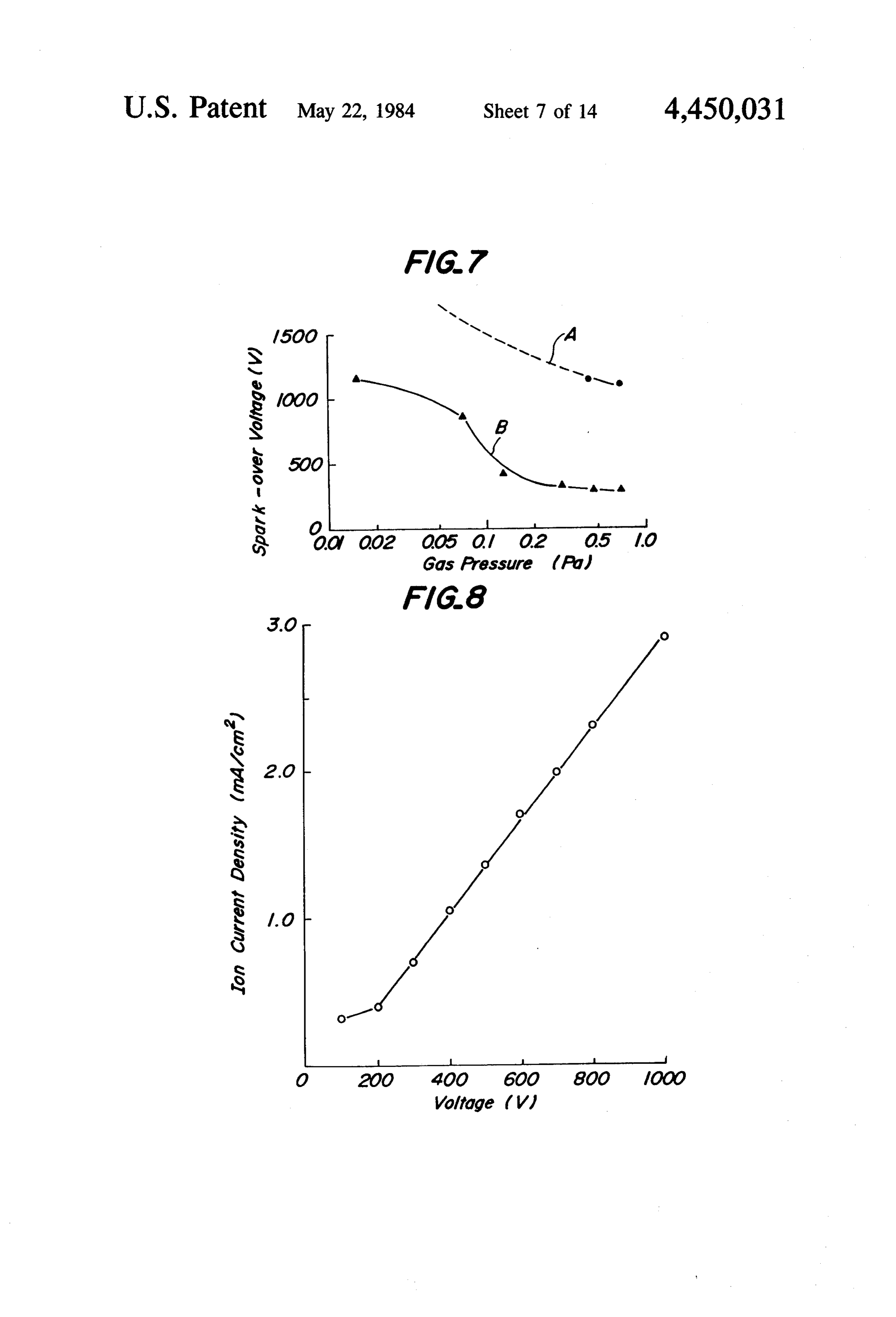
voltage) which causes spark-over in a uniform electric According to experiments, even when a voltage of field gap varies depending upon a type of gas, a gas 1,000 V is applied to the plasma formation chamber 1, pressure and a gap. For instance, in the case of argon 20 the operation of the ion source is stable, so that the gas at the pressure of 1 x 10³ Torr and when the gap is shower-like ion beam can be obtained in a stable man 100 cm, the spark-over voltage is about 200V. It is well ner. When a voltage of 500 V is applied, the thickness of known in the art that a gap and a spark voltage at which the plasma sheath is about 2 mm. Therefore, even when the spark discharge occurs are remarkably reduced the ion extraction electrode 7 is formed with apertures when electrons and ions exist or in the case of ultravio 25 3 mm in diameter, the sheath surface and the ion extrac let ray irradiation or heating by the light emission in tion electrode 7 are parallel with each other. As a result, plasma, so that the spark-over tends to occur very eas the shower-like ion beamm with a high degree of direc ily. A distance between the opposite electrodes of vari tivity can be obtained.
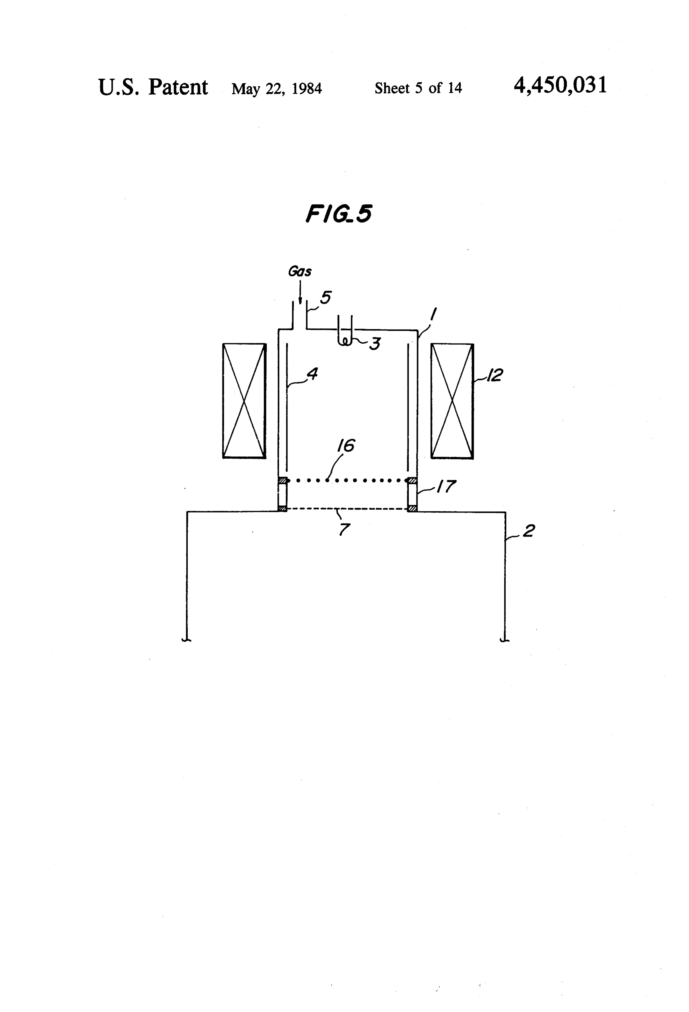
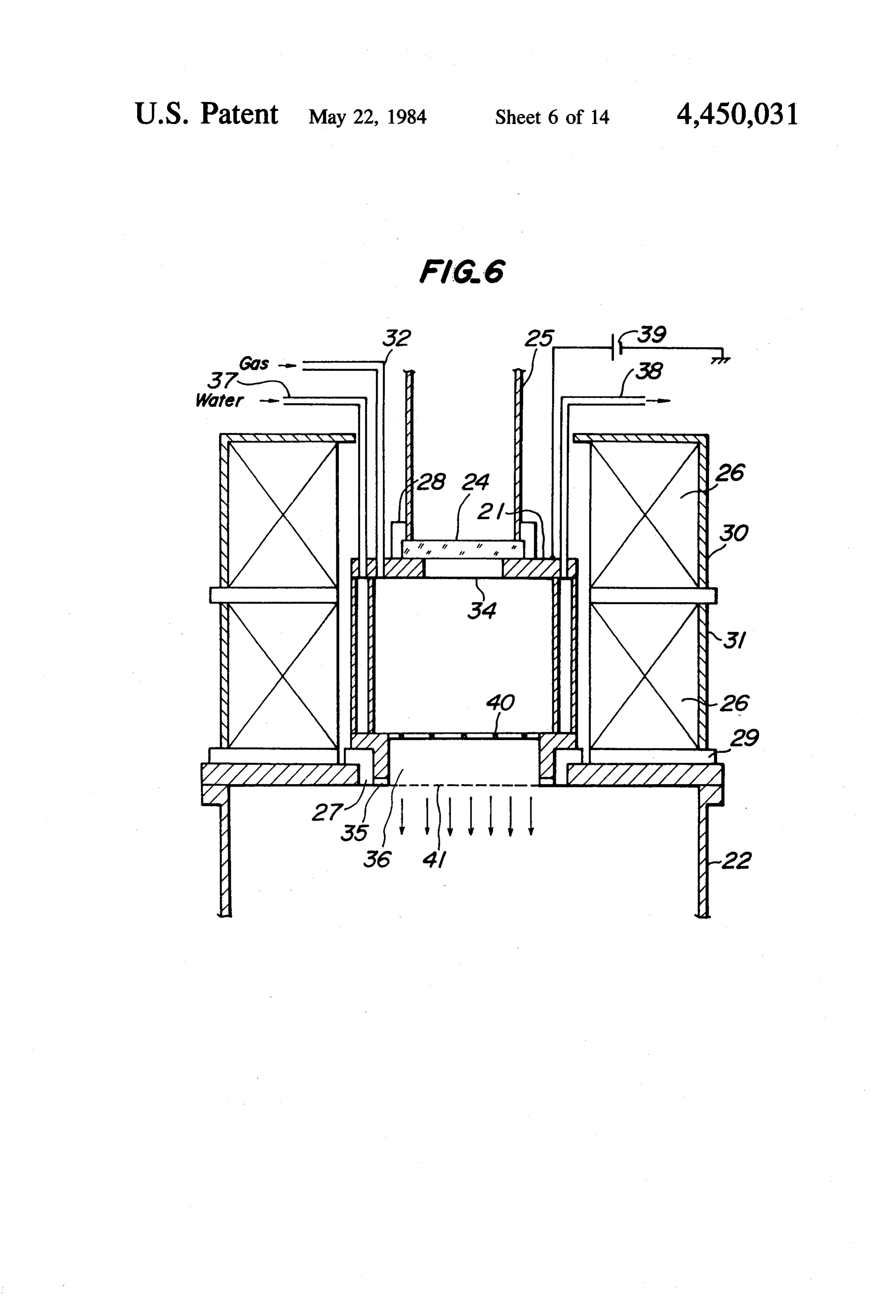
ous shapes can be defined by the length of an electric FIG. 6 shows a second embodiment of the present line of force perpendicular to an equipotential surface. 30 invention. Here, the inside structure of the specimen In view of the above consideration, it is very impor chamber 22 is omitted in order to focus on the structure tant to determine a grid shape and dimensions of the of the plasma formation chamber 21 and can be con shield electrode 16 and a distance between the shield structed as shown in FIG. 4 or 4A. In the second em electrode 16 and the ion extraction electrode 7, so that bodiment, electron cyclotron resonance caused by mi the plasma 10 can freely move toward the ion extraction 35 crowave is used to produce plasma. Reference numeral electrode 7 and that the length of the electric line of 21 denotes a plasma formation chamber; 22, a specimen force between the ion extraction electrode 7 and the chamber; 24, a microwave inctroducing window made shield electrode 16 is sufficiently shorter than a gap of fused quartz; 25, a rectangular waveguide; 26, a determined by Paschen's law. It is of course essential maentic coil; 27, 28 and 29, insulating members; 30 and that the distance between the shield electrode 16 and 40 31, magnetic shield members with a high permeability; the ion extraction electrode 7 is sufficiently greatly than 32, a gas inlet; 14, a microwave coupling window;35, an the thickness of the plasma sheath 14 so that the ion insulating spacer; and 36, a plasma transport chamber. extraction characteristics of the ion extraction electrode Reference numeral 37 denotes a cooling water inlet; 38, 7 are not adversely affected. a cooling water outlet; 39, an ion extraction power FIG. 5 shows a first embodiment of an ion shower 45 supply; and 40, a microwave reflection plate which also apparatus in accordance with the present invention. serves as a shielding electrode. The plasma formation Here, the inside structure of the specimen chamber 2 is chamber 21 defined by the shield electrode 40 is used as omitted in order to focus on the structure of the plasma a cylindrical cavity resonator so that the electric field is formation chamber 1 and can be constructed as shown increased in order to enhance the ionization. Reference in FIG. 4 or 4A. In the first embodiment, plasma is SO numeral 41 denotes a single ion extraction electrode produced by a thermionic cathode. Reference numeral which is substantially similar in construction to the ion 1 denotes a plasma formation chamber; 2, a specimen extraction electrode 7 as shown in FIG. 3. chamber; 3, a thermionic cathode; 4, an anode; 5, a gas Further, it is to be noted that there is arranged a inlet; 7, an ion extraction electrode; 12, a solenoid mag specimen table for supporting a specimen to be sub net; and 16, a shield electrode. Reference numeral 17 55 jected to etching or deposition or a target to be sput denotes an insulation spacer disposed between the elec tered and a specimen table for supporting a specimen to trodes 7 and 16. which the sputtered atoms are deposited in the speci Further, it is to be noted that there is arranged a men chamber 22.
specimen table for supporting a specimen to be sub In order to operate the ion source, for instance, C2F6 jected to etching or deposition or a target to be sput 60 is introduced through the gas inlet 32 to the plasma tered and a specimen table for supporting a specimen to formation chamber 21 at the pressure of 1 x 10 Torr. which the sputtered atoms are deposited in the speci The microwave at the frequency of 2.45 GHz, with a men chamber 2. power of 200 W is introduced through the rectangular In the mode of operation of the ion source, argon Ar, waveguide 25, the microwave introducing window 23 for instance, is introduced through the gas inlet 5 to the 65 and the microwave coupling window 34 into the plasma plasma formation chamber 1 at the pressure of formation chamber 21. Simultaneously, the magnetic 1.0x 10-Torr. The DC current of 21 A is supplied to field of 875 G is applied by the solenoid magnet 26, so the thermionic cathode 3, while a DC voltage of 19 V is that the electron cyclotron resonance is produced at 20 least at one portion in the plasma formation chamber 21. 3 mA/cm3 were obtained in a stable manner, respec in order to prevent the plasma formation chamber 21 tively. The ion extraction electrode 41 is considerably from being heated due to the production of the plasma, rigid so that even when the ions are extracted at such a cooling water flows from the inlet 37 to the outlet 38. high density as described above, the ion extraction elec The magnetic shield members 30 and 31 with a high trode 41 was prevented from being deformed as a result permeability surround the solenoid magnet 26 and of heating due to ion bombardment. cover the top thereof so that a divergent magnetic field In this way, anion shower apparatus according to the which is decreased in strength toward the ion extraction present invention can obtain an ion current stably in a electrode 41 is procured within the plasma formation wide voltage range. Accordingly, the present invention chamber 21. As a consequence, the ions in the plasma O is widely applicable to ion beam deposition in which a formation chamber 21 may easily move toward the ion relatively low voltage is used as well as ion beam sput extraction electrode 41. tering, ion etching or reactive ion etching in which a In order that the microwave power may be efficiently relatively high voltage is used.
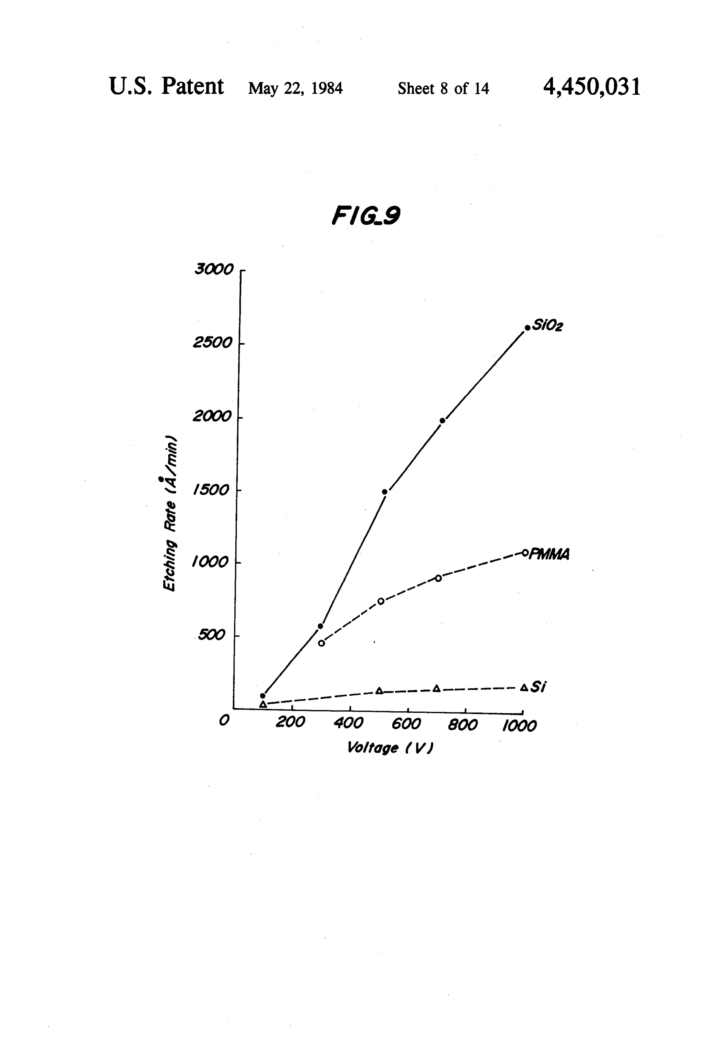
absorbed by the plasma in the plasma formation cham FIG. 9 illustrates the results of the experiments of the ber 21, the dimensions of the plasma formation chamber 15 selective etching of SiO2, in case that an etching is pro 21 is so determined as to satisfy the condition of micro cessed by the ion shower apparatus in accordance with wave cavity resonator. For instance, the inner height the present invention. That is, in FIG.9 there are shown and the inner diameter of the plasma formation chamber etching rates of various materials etched by the ion 21 are 200 mm and 170 mm, respectively, for the condi shower apparatus as shown in FIG. 6. The etching rate tion of microwave cavity resonator of (TE113). The 20 of Si, which is desired to be restricted, has a very small microwave is reflected back by the shield electrode 40 dependence on the ippi voltage. That is, the etching which also functions as the microwave reflector; that is, rate was about 150 A/min at 1,000 V. On the other the height of the microwave cavity resonator is defined hand, in the case of the etching of SiO2, the etching rate by the electrode 40. Furthermore, the insulating spacer is greatly dependent upon the voltage applied. Very 35 is interposed between the lower end of the plasma 25 efficient etching rates such as 1,000 A/min at 400 V and formation chamber 21 and the ion extraction electrode 2700 A/min at 1,000 V were obtained. The ratio of the 41 in a manner that the electric field produced by the etching rate of SiO2 to the etching rate of Si, which ion extraction electrode 41 is prevented from being reflects an etching selectivity, is about three at 100 V, extended to the interior of the plasma formation cham but the ratio increases to 10 at 400 V and to 18 at 1,000 ber 2. The shield electrode 40 which also serves as the 30 V. The etching rate of PMMA (polymethyl methacry microwave reflector consists of a stainless plate formed late) resist, which is used as an etching mask of a SiO2 with a matrix array of 18 mm)x18mm square apertures film, is an intermediate between the etching rate of spaced apart from each other by 20 mm. The ion extrac SiO2 and the etching rate of Si. The ratio of the etching tion electrode 41 consists of a stainless disk 180 mm in rate of SiO2 to the etching rate of PMMA was about 2 diameter and 0.5 mm in thickness. The stainless steel 35 to 400 V, which is satisfactory in practice. disk 41 is formed with apertures 2 mm in diameter FIG. 10 illustrates an ion shower distributions on the spaced apart from each other by 2.5 mm. The shield substrate or specimen table disposed substantially per electrode 40 serving as the microwave reflecting plate pendicular to the ion shower. The experimental results and the ion extraction electrode 41 are spaced apart shown were obtained under the conditions that a C2F6 from each other by 30 mm. The ion extraction electrode gas was used, a pressure in the plasma formation cham 41 is grounded and a DC voltage is applied to the ber was 0.28 Pa and a microwave power was 200 W. plasma formation chamber 21. The characteristic curve A shows the experimental FIG. T illustrates an effect of the shield electrode on result when the ion shower apparatus in accordance the spark-over voltage. The characteristic curve A is with the present invention was used, while the charac obtained when the distance between the shield elec 45 teristic curve B shows the experimental result when a trode 40 and the ion extraction electrode 41 was 30mm prior art ion shower apparatus having two electrodes in the arrangement shown in FIG. 6. The curve B is was used. According to the characteristic curve A, the obtained when the distance was 100 mm; that is, when variation in ion current density within the region of a the shield electrode 40 is eliminated in FIG. 6. In the diameter of 10 cm from the center of the table is 5%. latter case, in a normal operation pressure range from 50 Thus, a uniformion shower can be obtained with a large 0.08 Pa to 0.2 Pa and in a voltage range from 500 V to diameter. In contrast, the characteristic curve B shows 300 V, the spark-over occurs and the stable operation is that the ion shower is not uniform, since a distance not ensured. In the case of the characteristic curve A, in between the two electrodes varies due to the thermal the normal operation pressure range from 0.08 Pa to 0.2 deformations. While in the case of the curve B, instead Pa, the spark discharge occurs at a voltage higher than 55 of molybdenum which is less thermally deformed, a 1,000 V and the stable operation may be ensured over a stainless steel is used which is easily thermally de wide range of gas pressure. formed. As a result, the ion current density varied over FIG. 8 illustrates current characteristic curve ob a wide range. However, according to the present inven tained from experimental results when the ion shower tion, only one ion extraction electrode is used, so that apparatus of the present invention as shown in FIG. 6 is even if a stainless steel which easily tends to be ther used. The shield plate 40 which also serves as the micro mally deformed is used, a uniform ion shower can be wave reflecting plate was very effective in producing obtained without an influence of such deformation. stable plasma and in preventing the spark discharge. According to the present invention, only one ion Even when the voltage of 1,000 V was applied, the extraction electrode is used and it is preferable that the stable showerlike ion beam was produced. The ion 65 ion extraction electrode is made of silicon or carbon so density increases in linear proportion with the increase that the contamination of a specimen to be etched by of the voltage applied, as illustrated in FIG. 8. At 400 V metals forming the ion extraction electrode may be and 1,000 V, the ion current densities of 1 mA/cm and avoided. The reason is that even if the ion extraction 21 electrode 7 or 41 is sputtered by ions impinged thereon waveguide 25, while the magnetic field of 875 G is and the sputtered particles are deposited to the speci produced by the magnetic coil 26 so that the electron men being etched, this deposition does not lead to the cyclotron resonance may be produced at least one por contamination of the surface of the specimen in case of tion in the plasma formation chamber 21. The micro a semiconductor device consisting of materials in the 5 wave reflector 40 which also serves as the shield grid same category and the specimen is not contaminated by permits the free movement of the plasma to the ion foreign material. Thus, the silicon and carbon are very extraction electrode or grid 50, but reflects the micro effective in preventing specimens to be subjected to wave so that the microwave cannot pass through the etching or deposition from being contaminated with ion extraction grid 50. In the third embodiment, the metals. The silicon and carbon have high resistance to 10 shield grid 40 is formed by a metal plate having a plural heat, but are fragile. Accordingly, they have not been ity of 18 mm x 18 mm square apertures spaced apart used in a prior art ion shower apparatus where it is from each other by 20 mm and is spaced as art from the required to use a thin film and to form a plurality of fine ion extraction grid 50 by 30 mm. In order to facilitate apertures. In contrast, according to the present inven fthe absorption of the microwave by plasma, the inner tion, they can be advantageously used for the first time 15 diameter of the plasma formation chamber 21 is deter in an ion shower apparatus. mined to be 170 mm and the inner height between the As described above, according to the present inven top of the plasma formation chamber 21 and the shield tion, in an ion shower apparatus of the type in which electrode or grid 40 is determined to be 200 mm, so that ions produced in the plasma formation chamber are the plasma formation chamber 21 is in the form of a accelerated by the single ion extraction electrode and 20 microwave cavity resonator. In order to extract ions extracted into the etching chamber, the shield electrode from the plasma, a positive voltage is applied to the is disposed in the plasma formation chamber and spaced plasma formation chamber 21 by the power source 39, apart from the ion extraction electrode by a distance while the ion extraction electrode or grid 50 is which is sufficiently shorter than a distance defined by grounded.
Paschen's law and which is sufficiently greater than the 25 The ion extraction electrode or grid 50 is formed by thickness of the plasma sheath produced over the single a conductor member 52 and an insulating member 53. ion extraction electrode. As a result, a high voltage may The conductor member 52, for example, a conductor be applied to the single ion extraction electrode and a plate is formed by a stainless steel disk of 150 mm in high current density can be obtained stably. Therefore, diameter and 0.5 mm in thickness with apertures 51, when the ion shower apparatus in accordance with the 30 each of which has 2 mm in diameter and is spaced apart present invention is applied to the manufacture of semi from each other by 2.5 mm. The insulating member 53 conductor devices, an ion energy can freely be selected is comprised of a polyimide film of 0.3 mm in thickness. to the extent that a physical damage to a substrate is The polyimide film is formed by spraying polyimide allowable. Furthermore, the ion shower apparatus in over the upper surface of the conducting plate 52 on the accordance with the present invention is not only appli 35 side of contacting the plasma and then drying and heat cable to the manufacture of semiconductor devices but treating the sprayed polyimide. The insulating film 53 also equally applicable with a practical processing serves to electrically isolate the conducting plate 52 speed to other fields such as polishing or modification of from the plasma and may be regarded as in a floating surfaces which has been only accomplished by a chemi condition. Therefore, a negative potential is produced cal processing liquid or the like because of a low pro 40 in the insulating film in a self-regulation manner in ac cessing rate of an ion shower apparatus of prior art. cordance with the electron energy of plasma. Accord FIG. 11 shows a third embodiment of the present ingly, even though only one ion extraction grid 50 is invention in which an insulating member is provided on provided, it functions like the prior two-grid system. the surface of an ion extraction electrode. The surface is Therefore, the problem that high-energy electrons in on the side of the plasma formation chamber. Reference 45 the plasma flows into the ion extraction grid or elec numeral 50 denotes a single ion extraction electrode on trode 50 so that the grid or electrode 50 is locally heated the upper surface (that is, the surface in contact with may be avoided. Furthermore, even if a voltage as high plasma) of which an insulating member is provided. as 1,000 V is applied between the plasma formation Here, the inside structure of the specimen chamber 22 is chamber 21 and the ion extraction electrode 50, a show omitted in order to focus on the structure of the plasma 50 er-like ion beam can be obtained stably. Further, the formation chamber 21 and can be constructed as shown aperture 51 means an opening and may be in the form of in FIG. 4 or 4A. a various hole, like a round hole, an elliptical hole, a Further, it is to be noted that there is arranged a square hole, a rectangular hole or the like. The dimen specimen table for supporting a specimen to be sub sions of the aperture 51 refer to a size of the opening, for jected to etching or deposition or a target to be sput 55 instance, a diameter of the round hole, a minor axis of tered and a specimen table for supporting a specimen to the elliptical hole or the shortest side of the rectangular which the sputtered atoms are deposited in the speci hole.
men chamber 22. Next referring to FIGS. 12A and 12B, the detail of Further, cooling water is supplied from the water the ion extraction grid of the ion shower apparatus inlet 37 and then is discharged from the water outlet 38. shown in FIG. 11 will be described. In FIG. 12A, refer The ion extraction power source 39 is connected to the ence numeral 60 denotes plasma; 61, a plasma sheath; plasma formation chamber 21. 62, a plasma surface; and 63, an ion beam in the form of In operation, an etching gas such as C2F6 or C4Fs is a shower.
introduced to the plasma formation chamber 21 and the Ions in the plasma 60 reach the sheath interface 62 pressure within the plasma formation chamber 21 is and flow into the plasma sheath 61 toward directions maintained at 5x 10⁻⁵ through 5x 10⁻³ Torr. Micro perpendicular to the sheath interface 62. As a result, the wave of 2.45 GHz (TE10 mode) is introduced into the ions are imparted with an energy and a directivity de plasma formation chamber 21 from the rectangular pending upon the distribution and strength of the elec 22 thickness of 0.3 mm. The disk has apertures 51 which the side in contact with the plasma. Therefore, damage are 3 mm in diameter spaced apart from each other by to the ion extraction grid due to electrons and ions may 4 mm. The shield electrode 16 consists of a plurality of be minimized and the ion current extracted can be in molybdenum wires of 1 mm in diameter which are so creased. In addition, a shower-like ion beam can be arranged as to define square apertures of 5 mmX5 mm. 5 produced stably by the combination of the ion extrac The shield electrode 16 is spaced apart from the ion tion grid with the shield grid.
extraction grid 50 by 20 mm. The potential applied to Thus, the present invention provides an ion shower the shield grid 16 is equal to that applied to the plasma apparatus which is adapted for use in the etching or ion formation chamber 1. In experiments, an argon gas was beam sputtering process in the manufacture of semicon introduced through the inlet 5 into the plasma forma O ductor devices in which a high ion current must be tion chamber 1. The pressure in the plasma formation supplied in a stable manner with a low energy so that chamber 1 was maintained at 1.0X 10⁴ Torr. A DC the surface being etched is free from any defect layer in current of 21 A was supplied to the thermionic cathode which a crystal structure is disordered. 3 and a DC voltage of 19 V was applied to the anode 4, Various electrodes are investigated in order that an so that plasma was produced. A DC current of 1.0 A 15 ion shower apparatus is adapted for use in an etching was supplied to the magnetic coil 12 in order to enhance process in the manufacture of semiconductor devices. the ionization efficiency. The shower-like ion beam was The results are shown in FIG. 17. In the experiments, obtained by grounding the ion retraction grid 50, while C2F6 was used as an etching gas and was introduced to applying a positive DC voltage to the plasma formation a plasma formation chamber, the pressure in which was chamber 1. The experiments show that a shower-like 20 maintained at 0.28 Pa. The microwave power was 200 ion beam was produced stably, even if the voltage of W. In the case of ion etching, an electrode material is 1,000 V is applied. sputtered by ion bombardment and vaporized atoms While the embodiments have been explained in which and molecules are deposited to the etched surface of a the ion extraction grid 50 consists of the conductor plate semiconductor material. As a result of such a drawback, 52 made of stainless steel or molybdenum and the insu 25 an ion shower apparatus has not been used in the manu lating member 53 of polyimide film, it is to be under facture of semiconductor devices.
stood that the present invention is not limited to these In FIG. 17, a characteristic curve Ashows a relation materials and that other materials may be equally used. ship between an applied voltage and an ion current For instance, the conductor plate 52 may be made of density when the single ion extraction grid is made of carbon or silicon and the insulating member 53 may be 30 carbon. It is seen that as compared with a characteristic alumina or silicon dioxide such as working ceramic (for curve C of a two-electrode type apparatus of prior art, example, MACOR, a trademark of Corning Glass an ion current density higher than 1 mA/cm2 was ob Works). All these materials have a high melting point tained in case of the curve A, even at a low voltage. and are stable, even if they are exposed to plasma, so Even if a carbon electrode is sputtered, there arises no that their temperature becomes high. In addition, since 35 problem of contamination of the etched surface, be semiconductor devices are made of these materials, cause freon series gas (CFm) is normally used. A char even if these materials are sputtered by ions, the same acteristic curve B shows a relationship between an ap materials as the semiconductor devices are vaporized plied voltage and an ion current density when the insu and deposited on the surface of the semiconductor de lating film is deposited over the surface of the stainless vices. Thus, the surfaces of the semiconductor devices steel electrode. It is seen in the curve B that the ion are not contaminated. In the embodiments as shown in current density can be increased as compared with the FIGS. 11 and 16, if the ion extraction grid 50 consisting case of the characteristic curve A. In addition, there of the conductor plate 52 made of carbon and the insu arises no problem of the contamination of the etched lating member 53 made of silicon dioxide is used, then surface.
semiconductor materials could be subjected to etching 45 It is apparent that the present invention may equally or deposition without the contamination the specimen be applied to an ion shower apparatus in which a high surface. frequency discharge or the like is used to produce While in the above-described embodiments, a poly plasma for ionization. It is also apparent from the fore imide film has been deposited or otherwise formed on going that the present invention is applicable not only to the whole surface of a stainless steel or molybdenum 50 anion etching apparatus but also to anion beam sputter plate on the side in contact with plasma, it is to be un ing apparatus for forming a film by a deposition process derstood that when an ion extraction grid is combined utilizing ion beam sputtering technique. In this case, it is with a shield grid, an insulating film may be partially necessary to provide a holder for supporting a target at formed. This is preferable when it is desired that a large a given angle relative to an ion shower extracted from current is partially derived or that an effective ion 55 the plasma formation chamber and a specimentable for source dimensions are increased by improving the cur placing a specimen at such a position that the sputtered rent density distribution around the inner peripheral atoms are deposited to the specimen, portion of the ion source. Furthermore, the present invention is also applicable Further, the conductor plate of the ion extraction to an ion beam deposition process in which a raw mate grid may consist of other screens such as wire cloth rial gas such as SiH4 is introduced to the plasma forma with suitable openings, for instance, a molybdenum tion chamber in which ions to be deposited to form a screen with square openings, instead of the apertured film are produced, and then the ions are introduced to conductor plate as described above. the specimen chamber so as to form the film directly on As explained in the above, according to the present the specimen.
invention, a single ion extraction grid is used in an ion 65 While in the above embodiments the ion extraction shower apparatus. The ion extraction grid consists of a electrode or grid has been illustrated in the form of a conductor member and an insulating member closely planar plane, the ion extraction electrode may have a arranged on the surface of the conductor member on curved surface. If the ion extraction electrode is formed 23 tric field in the plasma sheath 61. When the thickness of with high energies do not impinge against the conduc the plasma sheath 61 is smaller than the dimensions of tor plate 52.
the aperture 51 of the ion extraction grid 60; that is, FIG. 15 illustrates measured results of ion current when the applied voltage is low, the sheath interface 62 characteristics, i.e., a relationship between an ion ex becomes convex upward with respect to the apertures traction voltage and an ion current density. Experimen 51, i.e., concave downward with respect to the direc tal data were obtained under the conditions that the tion of the travelling of the plasma. flow rate of a C2F6 gas was 10 cc/min and the gas pres If a voltage applied is increased so that the thickness sure was 2.0X 10⁻³ Torr. The characteristic curve A of the plasma sheath 61 is increased, or the dimensions 10 shows the prior art case in which two electrodes or of the apertures 51 are decreased no electric field is grids were spaced apart from each other by 1.5 mm, and extended to the insulating film 53 so that a potential at one of the two electrodes or grids on the side in contact with the plasma was floated. The microwave power the insulating film 53 is substantially the same as the was 300 W. The characteristic curve B shows an em plasma potential. Therefore, the thickness of the plasma bodiment according to the present invention, in which a sheath 61 is self-regulated corresponding to the electron energy upon the insulating film 53, whereas the thick 15 polyimide formed on insulating film 53 of 0.3 mm in thickness was the surface of the conductor plate 52 which ness of the plasma sheath above the apertures 51 is determined by a voltage applied between the plasma was in contact with plasma. The microwave power was formation chamber 21 (plasma 60) and the conductor 250It W. is seen from FIG. 15 that according to the present plate 52. Therefore, as shown in FIG. 12A, the sheath 20 invention, even though the microwave power is lower interface 62 becomes convex upward with respect to than that used in the prior art ion shower apparatus, a plasma 60. Under these conditions, the ion convergence high ion current density can be attained. Even at a is facilitated so that the ion current extraction efficiency relatively low voltage of 300 V, the practical ion cur and the directivity of the extracted ion current can be rent density of 1 mA/cm3 improved. As a result, the number of ions impinged 5 that the space between two was obtained. The reason is electrodes or grids in accor against the extraction grid 50 is decreased and even if dance with Child's law can be simulated by the thick the ions impinge against the extraction grid 59, only a ness of the plasma sheath. That is, the effects of the low voltage which is self-regulated corresponding to present invention are similar to those which can be the flow of electrons appears at the plasma sheath 61 attained when the spacing between the two electrodes above the insulating film 53. Since an energy of incident 30 or grids is extremely narrowed. Furthermore, the ef. ions is less as described above, the damage of the ion fects of the present invention can be attained by the ion extraction grid 50 due to the ion bombardment can be convergence due to the shape of the plasma sheath. reduced to a minimum. According to the present invention, even under the According to the present invention, as described conditions that a high ion current density more than 2.5 above, the insulating film 53 is formed on the conductor 35 mA/cm can be obtained, there is no damage observed plate 52 of the ion extraction grid 50, so that the ions to the ion extraction electrode or grid. with a high energy can be prevented from impinging When the ion extraction grid with the insulating film against the conductor plate 52. Furthermore, the effect is combined with the shield grid, reliability can be im of ion convergence can be expected by the plasma proved. However, if the insulating film on the ion ex sheath 61. These effects vary depending upon the thick 40 traction grid has defects such as pin holes, so that the ness of the plasma sheath 61 which is produced in a electric field produced by the ion extraction grids is self-regulation manner corresponding to the energies of extended to the plasma formation chamber, an abnor electrons impinged against the insulating plate 53, the mal discharge (spark-over) may be caused by such de thickness of the plasma sheath 61 produced in response fects. As a result, the generation of plasma becomes to the voltage applied to the conductor plate 52, the 45 unstable and the reliability drops. thickness of the conductor plate 52, dimensions of the In order to improve the reliability in operation, the apertures 51 and so on. When the conditions vary as shield grid must be so disposed that the electric field described above, the desired effect of the present inven produced by the ion extraction grid is locally confined tion can be attained by modifying the shape of the insu between the ion extraction grid and the shield grid. lating film 53. That is, even if the insulating film has some defects such For instance, in an example shown in FIG. 13, the as pin holes so that a part of the ion extraction grid is thickness of the plasma sheath 61 produced in a self. exposed to the plasma, an abnormal discharge and ad regulation manner on the insulating film 53 and the verse effects on the plasma formation chamber by the thickness of the plasma sheath 61 produced in response electric field can be avoided, whereby a shower-like ion to the application of a voltage to the conductor plate 52 55 beam can be obtained stably.
is small as compared with the dimensions of the aper FIG. 16 shows a fourth embodiment of the present tures 51 of the ion extraction grid 50. In this case, it is invention in which the present invention is applied to an preferable that the insulating film 53 is so formed that it ion source of the type in which plasma is produced by covers the side and top surfaces of the conductor plate the discharge by means of a thermionic cathode which 52. is known in the art as Kaufman type ion source. Here, FIG. 14 shows an example which is opposite to the the inside structure of the specimen chamber 2 is omit example shown in FIG. 13. That is, the thickness of the ted in order to focus on the structure of the plasma plasmasheath 61 is greater as compared with the dimen formation chamber 1 and can be constructed as shown sions of the apertures 51 of the ion extraction grid 50. In in FIG. 4 or 4A. . this case, it is preferable that the insulating film 53 is 65 An ion extraction grid 50 consists of, for example, a formed on the upper surface of the conductor plate 52 conductor plate 52 made of a molybdenum disk having and the width of the insulating film 53 is shorter than a thickness of 0.5 mm and a diameter of 100 mm and an that of the conductor plate 52 to the extent that the ions insulating member 53 of a polyimide film having a 24 to be convex at a given curvature over the entire sur tion chamber by means of discharge using a thermionic face thereof on the side of the plasma formation cham cathode.
ber, the ions are converged in a narrow region in the 3. An ion shower apparatus as claimed in claim 1, specimen chamber, so that an ion shower density is wherein said plasma is produced in said plasma forma easily enhanced. In contrast, if the ion extraction elec tion chamber by the electron cyclotron resonance ex trode is formed to be concave at a given curvature over cited by microwave.
the entire surface thereof on the side of the plasma 4. An ion shower apparatus as claimed in claim 1, formation chamber, the region that the ion shower is or wherein said ion extraction electrode is made of carbon irradiated uniformly can be easily made broader. If only silicon.
the peripheral portion of the ion extraction electrode is O 5. An ion shower apparatus as claimed in claim 1, made convex toward the plasma formation chamber, an wherein an insulating member is provided on the sur ion shower density in the periphery of the specimen face of said ion extraction electrode, said surface being table can be increased relative to the case where the on the side of said plasma formation chamber. 6. An ion shower apparatus as claimed in claim 2, peripheral portion is not made convex, and accordingly 15 wherein the region that the ion shower is irradiated uniformly is an insulating member is provided on the sur substantially extended. face of said ion extraction electrode, said surface being What is claimed is: on the side of said plasma formation chamber. 1. An ion shower apparatus comprising: 7. An ion shower apparatus as claimed in claim 3, wherein a plasma formation chamber in which a plasma is 20 face of said an insulating member is provided on the sur produced so as to produce ions; ion extraction electrode, said surface being a single ion extraction electrode disposed in one por on the side of said plasma formation chamber. tion of said plasma formation chamber and for wherein an insulatingapparatus 8. An ion shower member as claimed in claim 4, is provided on the sur extracting said ions from said plasma formation face of said ion extraction electrode, said surface being chamber so as to form an ion beam in the form of 25 on the side of said plasma formation chamber. shower; 9. An ion shower apparatus comprising: a specimen chamber in which the surface of a speci a plasma formation chamber in which a plasma is men is irradiated with said ion beam in the form of produced by the electron cyclotron resonance ex shower; and cited by microwave so as to produce ions; a shield electrode disposed in the vicinity of said ion 30 an ion extraction electrode disposed in one portion of extraction electrode in said plasma formation said plasma formation chamber and for extracting chamber and spaced apart from the thickness of the said ions from said plasma formation chamber so as plasma sheath produced over said ion extraction to form an ion beam in the form of shower; electrode, said shield electrode permitting the pas an insulating member provided on the surface of said sage of said plasma therethrough and preventing 35 ion extraction electrode, said surface being on the the electric field produced by said ion extraction side of said plasma formation chamber; and electrode substantially from extending to the re a specimen formation chamber in which the surface maining region of said plasma formation chamber. of a specimen is irradiated with said ion beam in the 2. An ion shower apparatus as claimed in claim 1, form of shower.
wherein said plasma is produced in said plasma forma k sk sk is k
Provenance
- Collection
- Patents citing this work
- Pages
- 24
- Method
- pdftotext (the PDF's own text layer) + pdftoppm 300dpi page scans
- Patent office record
- patents.google.com →
- Source
- Google Patents citing-documents table
- Assignee
- Nippon Telegraph & Telephone Public Corporation
- Published
- 1984-05-22
- Transcribed from
- patentimages.storage.googleapis.com →