

patent · US4464223A
Plasma reactor apparatus and method
7 August 1984
Text
Page 1scan →
United States Patent (19)
Gorin
54) plasma reactor apparatus and
Method
75 Inventor: Georges J. Gorin, Pinole, Calif. (73) Assignee: Tegal Corp., Novato, Calif.
52 U.S. C. .................................... 156/643; 156/646;
4,233,109 11/1980 Nishizawa ....................... 156/345 X
Tuneat
4,352,725 10/1982 Tsukada .......................... 204/192 E
Primary Examiner-William A. Powell
An improved plasma reactor apparatus and method are disclosed. Improved uniformity of etching and etch rate are achieved in a reactor through the use of electrodes powered at high and low frequencies. In one embodi ment of the invention the workpiece which is to be etched rests on an electrode powered at a low AC fre quency of about 100 KHz. A second electrode is pow ered at a high AC frequency of about 13.56 MHz. A third electrode is maintained at ground potential. High and low frequency AC fields acting on a reactant mate rial optimize the dissociation of the reactant material and the ion energy of the plasma generated reactant species.
11 Claims, 4 Drawing Figures
Common
Ground
Power supply
Power supply
Meter
Dc supply
Drawings
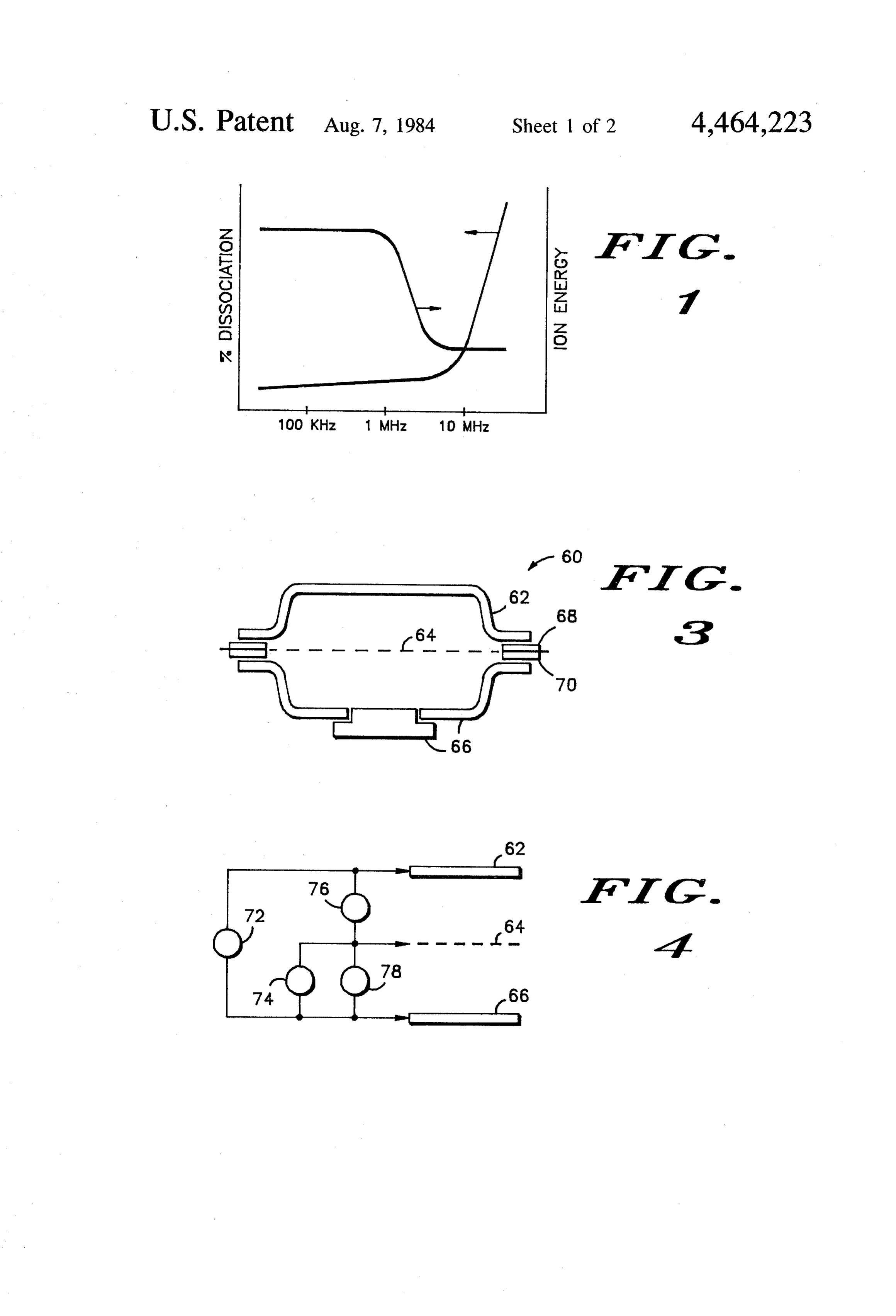
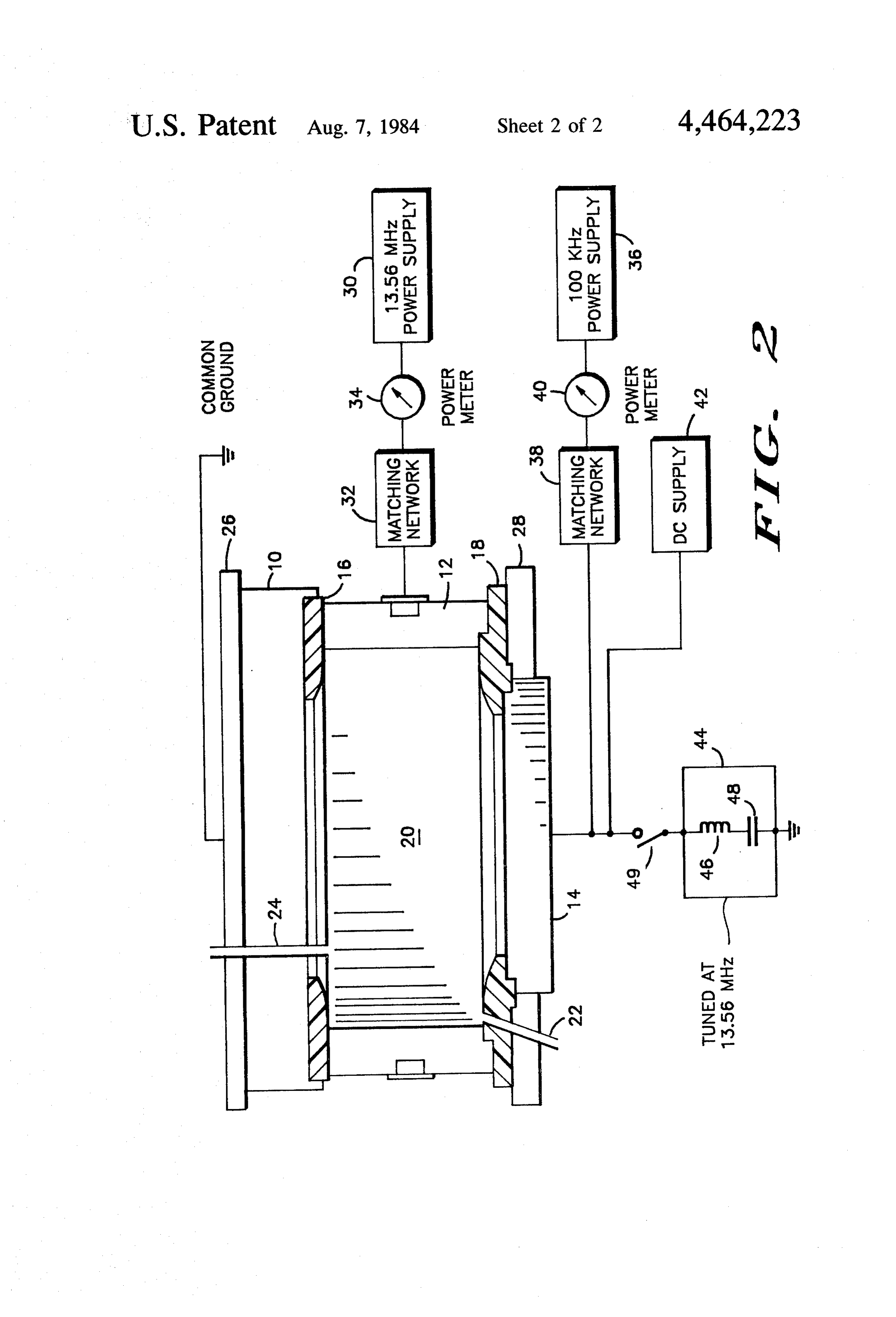
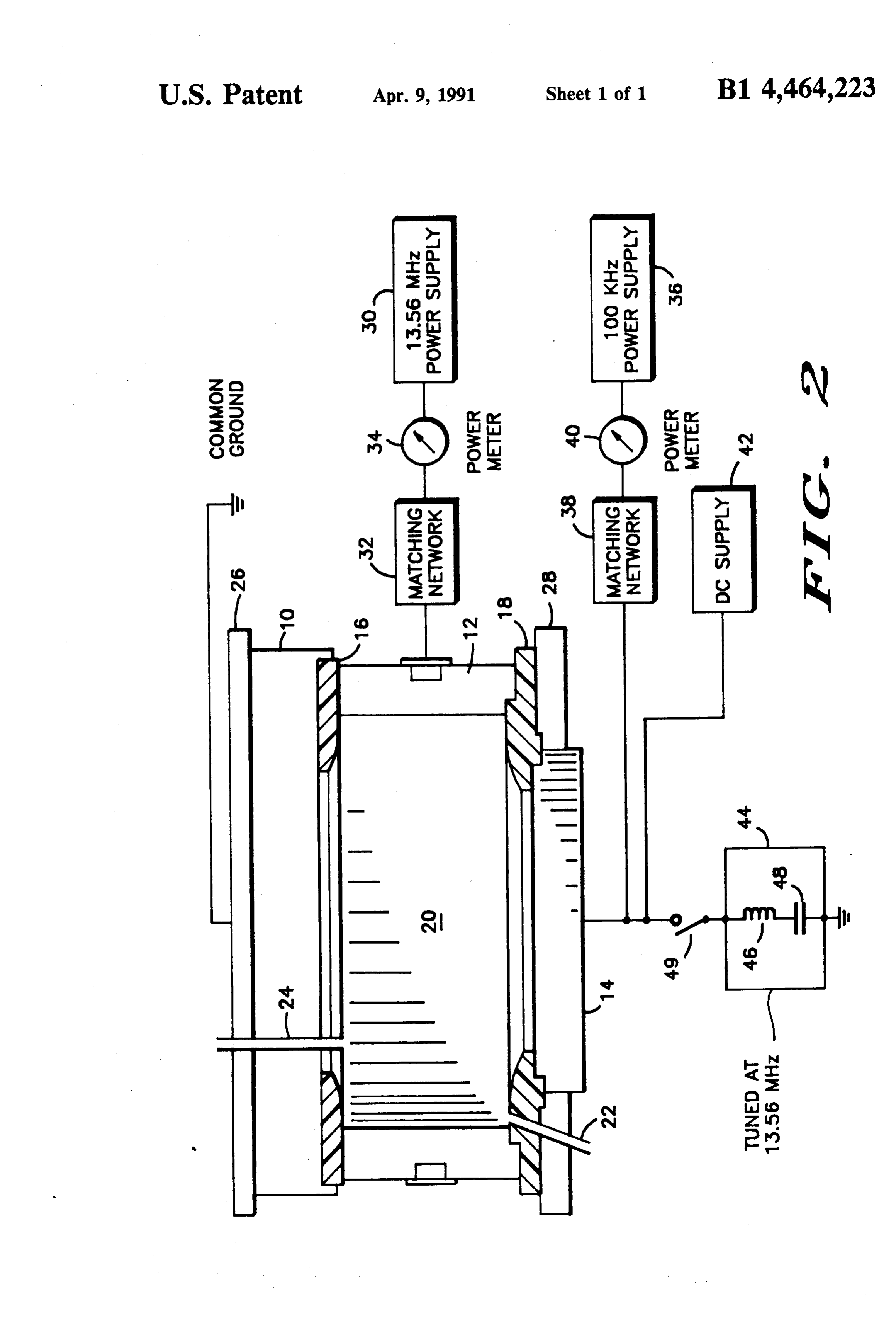
FIG. 4 illustrates coupling of the electrodes and
Page 2drawing sheetscan →
Page 3drawing sheetscan →
Page 4scan →
FIG. 4 illustrates coupling of the electrodes and
PLASMA REACTORAPPARATUS AND METHOD power supplies of the second embodiment of the appa ratus.
BACKGROUND OF THE INVENTION DETAILED DESCRIPTION OF PREFERRED This invention relates to an improved plasma reactor 5 EMBODIMENTS apparatus and method, and more specifically to a multi ple frequency plasma reactor apparatus and to a method andInplasma the nomenclature associated with plasma reactors processes, it is common to describe as "high for etching workpieces within that apparatus. frequency' any frequency greater than about 10 MHz. Plasma etching and reactive ion etching (RIE) have 10 "Low frequency" is correspondingly used to describe become important processes in the precision etching of any frequency less than certain workpieces such as in the fabrication of semi RF power applied to a about 1 MHz. The frequency of reactant gas has an appreciable conductor devices. Differences in the two processes, effect on the plasma that is generated from that gas. which generally can be carried out in the same equip FIG. 1 illustrates, for example, the effect of frequency ment, result from different pressure ranges employed 15 on the amount of dissociation that occurs in the reactant and from the consequent differences in mean free path gas making up the plasma. The dissociation remains low of excited reactant species. The two processes will until the frequency exceeds about 10 MHz. FIG. 1 also herein be referred to collectively as plasma etching. illustrates the effect of frequency on the energy of the Plasma etching is a "dry etching' technique and has a ions generated in the plasma. The ion energy is gener number of advantages over conventional wet etching in 20 ally high at low frequencies and falls off rapidly as the which the workpiece is generally immersed in a con frequency is increased. The amount of dissociation of tainer of liquid etchant material. Some of the advan the reactant gas and the energy of the ions within the tages include lower cost, reduced pollution problems, plasma have a marked effect on the uniformity of etch reduced contact with dangerous chemicals, increased ing and also upon the rate of etching. The uniformity of dimensional control, increased uniformity, improved 25 etch is a strong function of the high frequency power etch selectivity, and increased process flexibility. In while etch rate, for example in the case of oxide etching, existing plasma etch systems, however, it has not gener is a strong function of low frequency power. ally been possible to simultaneously achieve all of these A high degree of etch uniformity and a high etch rate advantages. A need therefore existed for equipment and are achieved, in accordance with the invention, through process which would make several of the foregoing 30 the use of a plasma reactor apparatus employing three advantages simultaneously attainable. electrodes in combination with both a high frequency It is therefore an object of this invention to provide power source and a low frequency power source. One an improved plasma reactor apparatus. embodiment of apparatus in accordance with the inven It is another object of this invention to provide an tion is illustrated in cross section in FIG.2. The appara improved plasma etch process which enhances process 35 tus includes a first electrode 10, a second electrode 12, flexibility. and a third electrode 14. The first and third electrodes It is another object of this invention to provide an are generally circular and the second electrode is ring improved plasma process which provides a higher de shaped. Ring-shaped ceramic insulators 16 and 18 pro gree of control over ion density and ion energy than vide electrical isolation between the first and second previously practical. and the second and third electrodes, respectively. To It is a still further object of this invention to provide gether the three electrodes and two ceramic rings an improved plasma reactor apparatus, and a process bound a generally cylindrical reaction volume 20. Al for practice in that apparatus, which provides an im though not shown, the electrodes can be provided with proved uniformity of etch, improved etch selectivity, temperature control means such as water cooling. and improved dimensional control. 45 A gas inlet 22 provides for the ingress of reactants to BRIEF SUMMARY OF THE INVENTION the reaction volume. A gas outlet 24 provides for the egress of reaction products from the reaction volume
The foregoing and other objects and advantages are under the influence of a vacuum pump (not shown). A achieved in the present invention through the use of a top plate 26 and a clamp ring 28 mechanically hold the multiple frequency plasma reactor apparatus. The 50 plasma reactor components together.
plasma reactor apparatus includes three electrodes. One Lower electrode 14 is adapted for movement in the of the electrodes is held at ground while the second is vertical direction. The electrode can be lowered to selectively coupled to a high frequency AC source and open the apparatus and to allow the placement of a the third is selectively coupled to a low frequency AC workpiece within reaction volume 20. The workpiece source. A plasma generated by the high and/or low 55 can be placed directly on the electrode, which functions frequency electric fields established between the elec as a workpiece holder, and then the electrode raised to trodes creates excited species of the reactants injected the closed position.
into the apparatus. The excited species act to precisely In accordance with the invention, a high frequency etch a workpiece positioned within the reactor. power supply 30 and a low frequency power supply 36
Brief description of the drawings
are coupled to the second and third electrodes, respec tively, so that high and low frequency electric fields can
FIG. 1 illustrates percentage dissociation and ion be established within the reaction volume to act upon energy as a function of plasma frequency; reaction gases which enter the reactor through inlet 22. FIG. 2 illustrates in cross section one embodiment of In a preferred embodiment of the invention the top plasma apparatus in accordance with the invention; 65 electrode 10 is coupled to ground. This electrode func FIG. 3 schematically illustrates a second embodiment tions as the common ground for the system, being the of plasma apparatus in accordance with the invention; ground reference for DC as well as high and low fre and quency AC supplies. The second electrode, the cylin 5 drical ring electrode 12, is coupled to a high frequency 70 electrically isolate the three electrodes from each AC power supply 30 through a matching network 32. other.
Power, including both forward and reflected power, is FIG. 4 schematically illustrates one way in which the monitored on a power meter 34. Lower electrode 14 is three electrodes can be powered. A high frequency coupled to a low frequency AC power supply 36 power supply 72 such as a supply at 13.56 MHz is cou through a matching network 38. Low frequency AC pled between electrodes 62 and 66. A low frequency power is monitored on a power meter 40. The high power supply 74, such as a supply having a frequency of frequency power supply is preferably at a frequency of about 100 KHz is coupled between electrodes 64 and about 13.56 MHz (a frequency allocated for industrial 66. In addition, DC supplies 76 and 78 are coupled uses by the FCC) and the low frequency power supply 10 between electrodes 62 and 64 and between electrodes 64 is preferably at a frequency of about 100 KHz. and 66, respectively. Each of the supplies can be turned In one embodiment of the invention the lower elec on or off or adjusted in power to create the desired trode is also coupled to a DC supply 42. Use of a DC plasma and to establish the desired DC bias on one or . power supply allows the amount of DC biasing induced 15 more electrodes.
by the plasma to be changed, independently of pressure The following are non-limiting examples which serve or power. to further illustrate practice of the invention and to In a still further embodiment of the invention, a series disclose preferred embodiments contemplated by the circuit 44, including, for example, an inductor 46 and inventor.
capacitor 48, tuned to the frequency of high frequency EXAMPLE I power supply 30, is coupled between lower electrode 14 A plurality of silicon wafers were thermally oxidized and ground. Switch 49 permits the selective coupling of to grow a silicon dioxide layer about 500 nm in thick series circuit 44 to electrode 14.
During operation of the apparatus, in accordance ness. Over the oxide layer was formed a layer of poly. crystalline silicon, heavily doped with phosphorous and with the invention, a workpiece, such as a semiconduc 25 having a thickness of about 500 nm. A patterned photo tor wafer, is placed on electrode 14 and the reaction resist etch mask was volume is evacuated to a desired low pressure. Reactant crystalline silicon. Thethen formed on the layer of poly wafers were divided into groups gases are then admitted to the reaction chamber and the for the patterned plasma etching of the polycrystalline power supplies are energized. Either one or both AC layer in a reactor as illustrated in FIG. 2. The polycrys power supplies can be energized, with or without the 30 talline layer was first etched in a mixture DC supply. Either AC supply creates a plasma within 10% CCl3F. The pressure in the reactor wasofmaintained SF6 plus the reaction volume so that excited species of the reac at 0.25 torr. The AC power between the top and side tant gas are created. Energizing high frequency supply electrodes was maintained at 100 watts CW at 13.56 32 establishes an electric field which exists principally MHz. The polycrystalline silicon was etched until end between upper electrode 10 and side electrode 12. Ener 35 point was detected, approximately 40 seconds. The gizing low frequency power supply 36 creates a low polycrystalline silicon layer was then given an overetch frequency field which exists principally between lower in CCl3F for about 18 seconds. During the overetch the electrode 14 and upper electrode 10. The combination high frequency power was maintained at 100 watts. One of the two fields within the reaction volume and in group of wafers was overetched with an additional DC proximity to the workpiece located on the lower elec 40 bias of 100-150 volts applied to the wafer support elec trode causes maximum dissociation of the reaction gas trode; one group was overetched without an additional as well as imparting a high ion energy to the ions within DC bias. Wafers were examined after the etching. the plasma. Those wafers overetched without a DC bias exhibited The selective use of series circuit 44 by the closing of undercutting of the photoresist mask and a negative switch 49 has two effects. First, the tuned series circuit, 45 slope in the etched openings. That is, etched openings which effectively places the lower electrode 14 at were narrower at the top of the polycrystalline silicon ground with respect to the high frequency supply, layer than at the bottom. Those wafers etched with a changes the electrode area ratio between the high fre DC bias exhibited a decrease in undercutting and an quency electrode and the ground electrode. This affects increase in etched opening profile control. Additional the plasma sheath potential above the wafer without 50 groups of wafers were etched with a low frequency physically changing the reactor. Second, coupling the (100 KHz) supply coupled to the wafer support elec series tank circuit to the lower electrode selectively trode. The low frequency plasma increased the aniso couples the high frequency supply to the workpiece trophy of the polycrystalline silicon etch, but the etch itself. This allows the optimizing of etch rates and etch selectivity of polycrystalline silicon over silicon dioxide selectivity for certain films. For example, the etch rate 55 decreased.
of silicon is high at low frequencies and drops off rap EXAMPLE II idly at high frequencies. In contrast, aluminum etches only slowly at low frequencies but etches rapidly at A plurality of silicon wafers were thermally oxidized high frequencies. Thus, by selectively turning on or off to grow a 500 nm thick layer of silicon dioxide. A layer the low frequency power supply and by selectively 60 of aluminum plus 4% copper was applied over the sili coupling or uncoupling the series circuit, the workpiece con dioxide to a thickness of 1000 nm. A patterned can be exposed to a high frequency, low frequency, or photoresist mask was formed over the Al/Cu layer. The mixed frequency plasma. wafers were divided into two groups for the etching of FIG. 3 schematically illustrates a further embodiment the alumimum. Both groups were etched in a CCl4 of the invention. In this embodiment a plasma reactor 60 65 plasma at 0.2-0.3 torr in a reactor as illustrated in FIG. includes a first top electrode 62, a screen electrode 64, 2. One group was etched using only a 13.56 MHz and a bottom electrode 66. The bottom electrode can plasma with the high frequency plasma maintained at also function as a workpiece holder. Insulators 68 and 125 watts CW. The second group was etched using an 6 additional 100 KHz power supply maintained at 50-100 reactant gases, and applications of the invention. It is watts CW. The Al/Cu film etched about 30% faster intended that all such variations and modifications be when using the two power supplies than when using the included within the appended claims. high frequency power supply alone. In addition, using I claim:
the two power supplies together resulted in a cleaner 5 1. A reactor apparatus including a reaction volume resultant wafer with less residue than when using the into which reactants are injected and from which reac high frequency supply alone. tion products are exhausted, and in which said reactants
Example iii
are acted upon by electric fields to form a plasma thereof, said apparatus comprising: first, second, and
A number of silicon wafers were thermally oxidized 10 third electrodes, said first electrode coupled to electri to grow a 500 nm layer of silicon dioxide. A patterned cal ground, said second electrode selectively coupled to photoresist mask was formed over the oxide layer. The a high frequency source of AC power, and said third oxide layer was pattern etched in a CF4 plasma at about electrode selectively coupled to a low frequency source 0.050 torr in a plasma apparatus as illustrated in FIG. 2. of AC power.
The wafers were divided into groups for etching. The 15 2. The reactor of claim 1 wherein said third electrode first group was etched in a high frequency plasma (13.56 is further coupled to a source of DC power. MHz, 200 watts). The etch rate of the oxide was mea 3. The reactor of claim 1 wherein said third electrode sured to be 9.5 nm per minute. The second group was is adapted for holding a workpiece.
etched in a low frequency plasma (100 KHz, 200 watts). 4. The reactor of claim 3 wherein said third electrode The etch rate of the oxide in the low frequency plasma 20 is temperature controlled.
was measured to be 93.7 nm per minute. The third 5. The reactor of claim 3 wherein said third electrode group was etched in a high frequency/low frequency is water cooled.
plasma (13.56 MHz, 200 watts; 100 KHz, 200 watts). 6. The reactor of claim 1 further comprising means The etch rate was measured to be 122.7 nm per minute. having a low impedance at the frequency of said high Additional groups were etched as above, but with a DC 25 frequency source selectively coupled between said third bias of up to 500 volts applied to the wafer holder elec electrode and electrical ground. trode to reduce the natural DC bias established by the 7. A plasma reactor apparatus comprising: first, sec plasma. The wafers etched with the additional DC bias ond, and third electrodes; a first insulator electrically were found to have improved photoresist integrity and separating said first and second electrodes; a second improved uniformity. 30 insulator electrically separating said second and third
Example iv
electrodes; said electrodes and said insulators positioned to bound a reaction volume; means for admitting reac
Wafers were prepared and etched as in Example III tants to said reaction volume and for removing reaction except that the AC power supplies were pulsed, with products from said reaction volume; a first high fre the high and low frequency power supplies operated 35 quency AC power supply selectively coupled to said alternately. One AC supply was operated for 1 msec., second electrode; a second low frequency AC power AC power off for 0.2 m.sec., the other AC power supply supply selectively coupled to said third electrode; and was operated for 1 m.sec., AC power off for 0.2 msec., an electrical ground coupled to said first electrode. and so on. The etch rates of the oxide were nearly the 8. A method for etching a workpiece positioned in a same as with continuously operated supplies and there 40 plasma reactor apparatus which comprises the steps of: was less attack of the photoresist. Very importantly, providing first, second, and third electrodes in said harmonics were not generated as is possible when si apparatus; injecting a reactant gas into said apparatus; multaneously operating the two AC supplies. and creating a reactant gas plasma by selectively apply Thus it is apparent that there has been provided, in ing a high frequency AC field between said first and accordance with the invention, an improved plasma 45 second electrodes and a low frequency AC field be reactor apparatus and method which fully meet the tween said first and third electrodes.
objects and advantages set forth above. While the in 9. The method of claim 8 further comprising the step vention has been described and illustrated with refer applying a DC bias between said first and third elec ence to specific embodiments thereof, it is not intended trodes.
that the invention be so limited. Those skilled in the art, 50 10. The method of claim 8 wherein said high fre after consideration of the foregoing description, will quency and said low frequency AC fields are pulsed. recognize that many variations and modifications are 11. The method of claim 10 wherein said low fre possible which still fall within the broad scope of the quency and said high frequency AC fields are alter invention. Such variations include the particular shape nately applied. k se k is sk of the electrodes, positioning of gas inlets and outlets, 55
Page 7scan →
REEXAMINATION CERTIFICATE (1447th)
United States Patent (19)
Gorin 45 Certificate Issued Apr. 9, 1991 (54) PLASMA REACTOR APPARATUS AND (56) References Cited METHOD U.S. PATENT DOCUMENTS 2,468,174 4/1949 Cotton ................................. 204/312 3,458,817 7/1969 Cooper et al. ...................... 325/180 75) Inventor: Georges J. Gorin, Pinole, Calif. FOREIGN PATENT DOCUMENTS
73 Assignee: Tegal Corp., Novato, Calif. OTHER PUBLICATIONS Chapman, "Triode Systems for Plasma Etching', IBM
Reexamination Reqsist: Technical Disclosure Bulletin, vol. 21, No. 12, May No. 90/001,809, Jul. 14, 1989 1979, pp. 5006-5007.
No. 90/001,674, Dec. 20, 1988 "Triode Plasma Etching' Minkiewicz and Chapman,
Reexamination Certificate for:
Patent No.: 4,464,223 Primary Examiner-William A. Powell Issued: Aug. 7, 1984 57 ABSTRACT Appl. No.: 538,593 An improved plasma reactor apparatus and method are Filed: Oct. 3, 1983 disclosed. Improved uniformity of etching and etch rate are achieved in a reactor through the use of electrodes powered at high and low frequencies. In one embodi 51) Int. Cl....................... H01L 21/312; B44C 1/22; ment of the invention the workpiece which is to be CO3C 15/00; C23F 1/02 etched rests on an electrode powered at a low AC fre 52 U.S. C. .................................... 156/643; 156/646; quency of about 100 KHz. A second electrode is pow 156/345; 204/192.32; 204/192.34; 204/298.34 ered at a high AC frequency of about 13.56 MHz. A 58) Field of Search ............... 156/345, 643, 646, 653, third electrode is maintained at ground potential. High 156/656, 657, 659.1, 662, 665; 118/50.1, 728, and low frequency AC fields acting on a reactant mate 620, 625; 427/38, 39; 204/164, 192.32, 192.35, rial optimize the dissociation of the reactant material 298 TT, 298 E, 298 EP, 298 PP, 298 EM; and the ion energy of the plasma generated reactant 219/121.4, 121.41, 121.43, 121.52, 121.53 species.
Common
Nynyny
Matching
Network
Power
Power supply
Meter
Matching
Nework
Power supply
Meter
Dc supply
Tuned at 42
Page 8drawing sheetscan →
Page 9scan →
5. The reactor of claim 3 1 wherein said third
REEXAMINATION CERTIFICATE electrode is adapted for holding a workpiece and is water cooled.
ISSUED UNDER 35 U.S.C. 307 6. The reactor of claim 1 further comprising A
The patent is hereby amended as
5 reactor apparatus including a reaction volume into which
Indicated below
reactants are injected and from which reaction products are exhausted, and in which said reactants are acted upon by electric fields to form a plasma thereof, said apparatus
Matter enclosed in heavy brackets I appeared in the comprising patent, but has been deleted and is no longer a part of the 10 first, second, and third electrodes, patent; matter printed in italics indicates additions made said first electrode coupled to electrical ground, to the patent. said second electrode selectively coupled to a high fre quency source of AC power, and
AS A RESULT OF REEXAMINATION, IT HAS said third electrode selectively coupled to a low frequency BEEN DETERMINED THAT: 15 source of AC power and means having a low impedance at the frequency of
The patentability of claims 8–11 is confirmed. said high frequency source selectively coupled Claim 3 is cancelled. between said third electrode and electrical ground. Claims 1, 2 and 4-7 are determined to be patentable as 20 piece Ain plasma 7. reactor apparatus for treating a work a glow discharge comprising:
amended.
New claims 12-15 are added and determined to be pat first, second, and third electrodes separated by insula entable.
tors for defining a reaction volume in which said work piece is located a first insulator electrically separating said first and 1. A reactor apparatus including a reaction volume 25 second electrodes;
into which reactants are injected and from which reac a second insulator electrically separating said second tion products are exhausted, and in which said reactants and third electrodes; are acted upon by electric fields to form a plasma said electrodes and said insulators positioned to thereof, said apparatus comprising: bound a reaction volume; first, second, and third electrodes, 30 means for admitting reactants to said reaction volume said first electrode coupled to electrical ground, and for removing reaction products from said reac said second electrode selectively coupled to a high tion volume;
frequency source of AC power, and a first high frequency AC power supply selec said third electrode selectively coupled to a low fre tively coupled to between said first electrode quency source of AC power, and 35 and said second electrode; wherein one of said electrodes is adapted for holding a a second low frequency AC power supply selec workpiece. tively coupled to between said first electrode 2. The reactor of claim 1 wherein said third elec and said third electrode; and trode is further coupled. A reactor apparatus including a an electrical ground coupled to said first electrode, reaction volume into which reactants are injected and from said first and second power supplies producing different which reaction products are exhausted, and in which said frequencies respectively above about 10 Mhz and reactants are acted upon by electric fields to form a plasma below about 1 Mhz for causing a glow discharge in said volume.
thereof, said apparatus comprising 12. The reactor of claim 1 wherein said first electrode is first, second, and third electrodes, 45 adapted for holding a workpiece. said first electrode coupled to electrical ground, 13. The reactor of claim 1 wherein said second electrode said second electrode selectively coupled to a high fre is adapted for holding a workpiece.
quency source of AC power, and 14. The reactor of claim 1 wherein said third electrode is said third electrode selectively coupled to a low frequency adapted for holding a workpiece.
source of AC power and to a source of DC power. 50 15. The reactor of claim 1 wherein said second electrode 4. The reactor of claim 3 1 wherein said third is cylindrical and one of said first and third electrodes is electrode is adapted for holding a workpiece and is tem adapted for holding ask workpiece.
perature controlled.
Provenance
- Collection
- Patents citing this work
- Pages
- 9
- Method
- pdftotext (the PDF's own text layer) + pdftoppm 300dpi page scans
- Patent office record
- patents.google.com →
- Source
- Google Patents citing-documents table
- Assignee
- Tegal Corp.
- Published
- 1984-08-07
- Transcribed from
- patentimages.storage.googleapis.com →