

patent · US4610748A
Apparatus for processing semiconductor wafers or the like
9 September 1986
Text
Page 1bibliographic recordscan →
Engle et al.
(54) APPARATUS FOR PROCESSING
SEMCONDUCTOR WAFERS OR THE LIKE
75 Inventors: George M. Engle, Scottsdale; Richard S. Rosler, Paradise Valley, both of
Ariz.
(73) Assignee: Advanced Semiconductor Materials of America, Inc., Phoenix, Ariz.
Int. Cl." .......................... B44C 1/22; C23F 1/00;
(52) U.S. C. ................................... 156/345; 118/50.1;
4,78,877 12/1979 Kudo .............................. 156/646 X
4,233,109 11/1980 Nishizawa ........... . . . . . . . . . . . . 156/345 X
Primary Examiner-William A. Powell
Attorney, Agent, or Firm-Harry M. Weiss & Associates
A disk boat assembly for holding workpieces to be processed within a chemical reaction processing appa ratus during the chemical vapor process. The boat as sembly includes a pair of electrically conductive rail members held rigidly and radially apart between two dielectric end holding members that electrically isolate the two rail members. A plurality of disk like plates are connected respectively to the two rail members and are interleaved such that adjacent disk plates are electri cally isolated. Each disk plate includes pairs of bores formed therein with each pair extending radially out ward from the center of the disk. Insertable pins are placed in a respective pair of bores, the distance there between of which can be extended by insertion in an additional pair of bores lying further from the center of the disk so that variable diameter workpieces can be held on the broad surfaces of each disk plate. 4. Claims, 6 Drawing Figures
Drawings
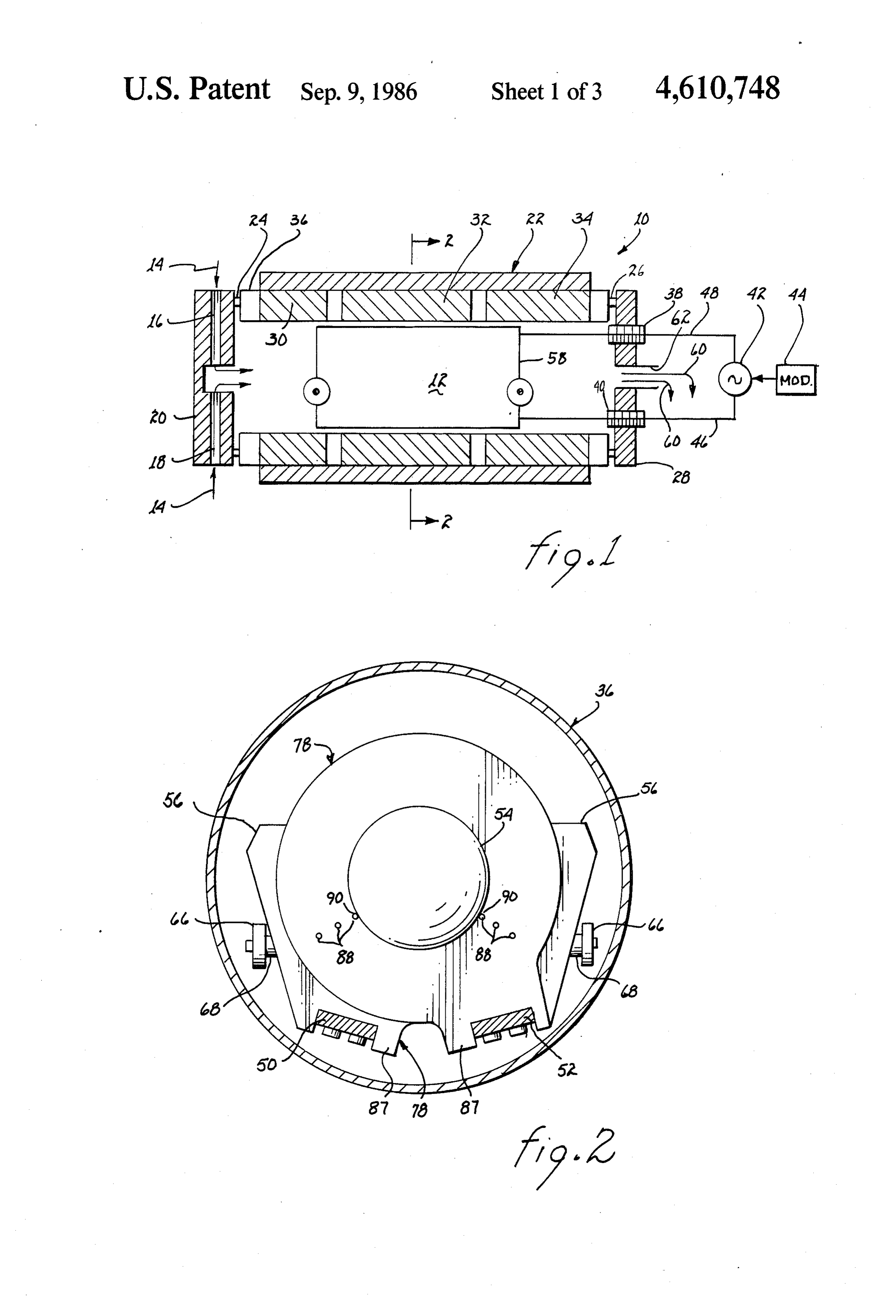
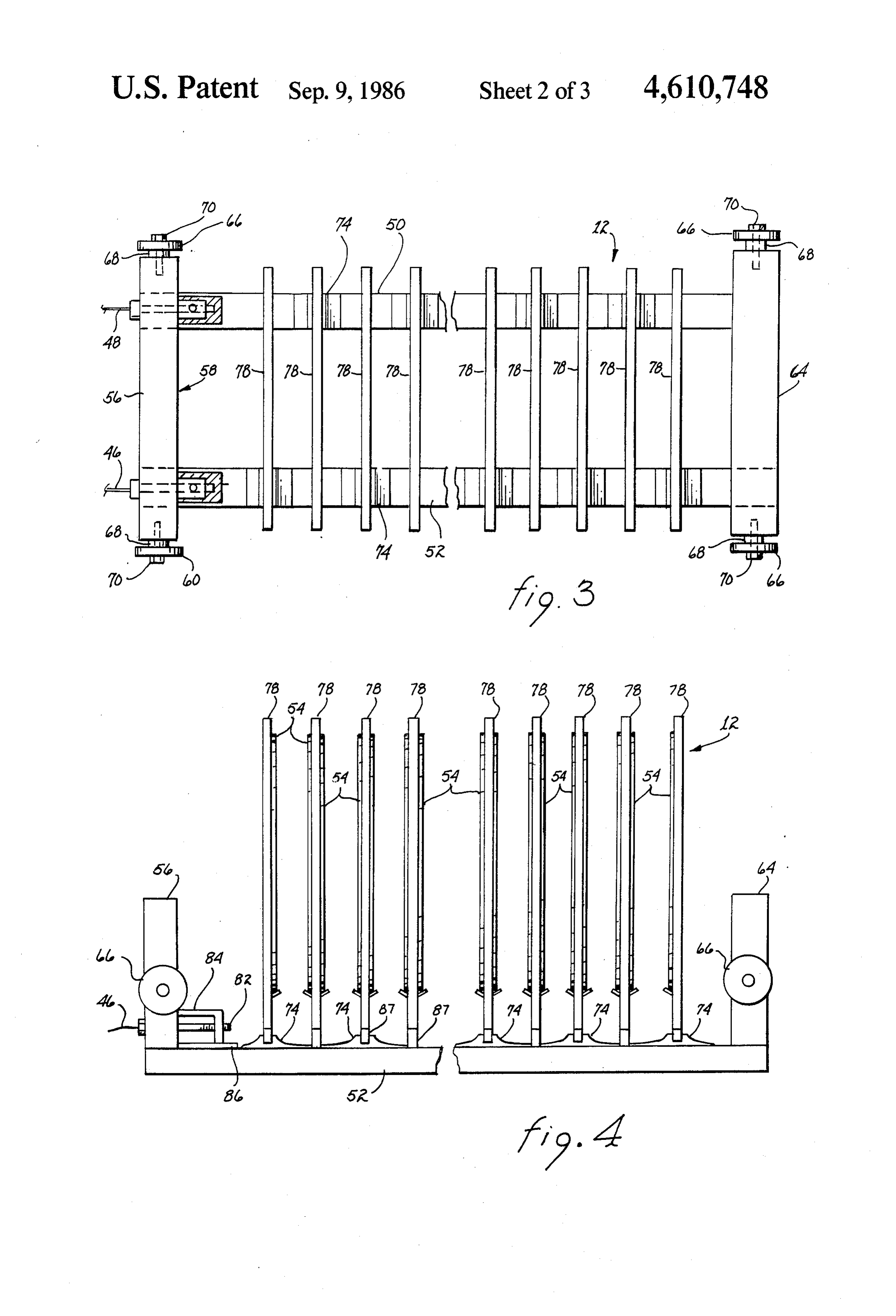
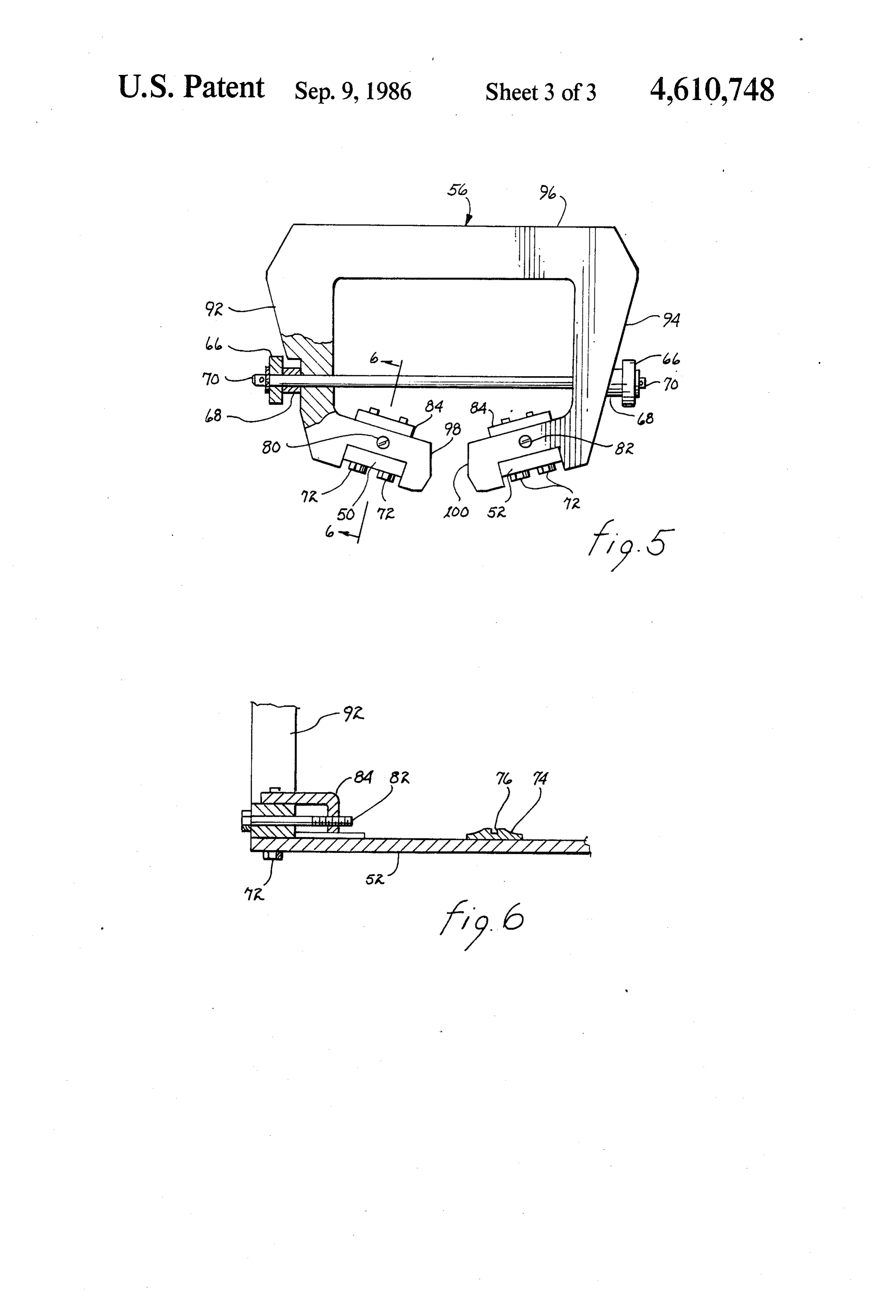
FIG. 5 is a plan end view of the one end of the boat
Page 2drawing sheetscan →
Page 3drawing sheetscan →
Page 4drawing sheetscan →
Page 5scan →
components, higher deposition rates and the use of less
APPARATUS FOR PROCESSING peak power are achieved.
SEMCONDUCTOR WAFERS OR THE LIKE In accordance with the above and other objects, there is disclosed a boat assembly comprising holding
BACKGROUND OF THE INVENTION 5 ends which rigidly support a pair of conductive rails The present invention relates to processing of semi therebetween, each rail having a plurality of interleaved conductor wafers and, more particularly, to a boat as disk plate assemblies held thereto with each rail being sembly used to hold semiconductor wafers or the like electrically isolated from the other and the disk plate within externally excited, chemical reaction systems assemblies having adjustable holding assemblies for wherein the reactant flows over the wafers or work 10 holding workpieces.
pieces that are held with their broad surfaces in perpen A feature of the invention is that different circumfer dicular to the flow of the reactant. ence workpieces can be held on opposite surfaces of the Plasma enhanced chemical vapor reactors are known disk plate assemblies each with its broad surface being in the art wherein the plasma reactant gas orgasses flow 15 perpendicular to the flow of a gaseous reactant when across serially arranged workpieces perpendicular to the boat assembly is removably inserted in an externally the broad surfaces of the workpieces. For instance, U.S. excited chemical reaction processing apparatus with Pat. No. 4,401,507, which is incorporated herein by each of the rails being executed by an alternating RF reference made thereto, is exemplary of the type of power source.
plasma chemical vapor reactor to which the present 20 The features and advantages of the present invention invention is applicable. The chemical reactor systems of will be apparent from the following description of the the type disclosed in the U.S. Pat. No. 4,401,507, utilize preferred embodiment as illustrated in the accompany an evacuable tabular envelope retained in a furnace. A ing drawings.
boat assembly that is removably inserted into the tabu lar envelope is used to hold workpieces perpendicular BRIEF DESCRIPTION OF THE DRAWINGS to the flow of the gas reactants that are passed through 25
FIG. 1 is a partial schematic and block diagram longi the tabular envelope during the depositing process of tudinal sectional view of a plasma enhanced reaction the workpieces. Of great concern in these chemical system including the assembly of the present invention; vapor reactor systems is the degree of process uniformi FIG. 2 is a cross-sectional transverse view of the ties achievable. It is desirable to maintain the deposit 30 structure of FIG. 1 taken along the direction of arrows thickness of film properties of the workpieces processed 2-2;
in the chemical reactors to maximum of 5% from one FIG. 3 is a top plan view in fragmentory of the boat end of the loaded boat assembly to the other. In addi assembly illustrated in FIG. 1; tion, it is desirable to be able to process as many work pieces as possible during each chemical vapor deposi of FIG. 3;is a side elevational view of the boat assembly FIG. 4 tion process. 35
FIG. 5 is a plan end view of the one end of the boat
Thus a need exists for an improved apparatus which assembly of FIG. 3; and can be utilized in contemporary plasma enhanced chem ical vapor deposition reactors that can maintain the end of theisboat
FIG. 6 a cross-sectional view of the portion of the process uniformities below --5% while allowing a of arrows 6-6.assembly of FIG. 4 taken in the direction larger number of workpieces to be processed at one 40 time than is presently possible with conventional boat DETAILED DESCRIPTION OF THE assemblies presently available. INVENTION SUMMARY OF THE INVENTION Referring to FIG. 1 there is shown a plasma en Accordingly, it is an object of the present invention 45 hanced chemical vapor processing apparatus 10 of the to provide an improved boat apparatus for use in the type and operation that is fully described in U.S. Pat. processing of workpieces. No. 4,401,507 issued to George Engle on Aug. 30, 1983. It is another object of this invention to provide an Apparatus 10 has not been completely illustrated as its apparatus for improved uniformity in an externally structure and operation is well known to those in the excited chemical reaction process. 50 art, for instance, the aforementioned U.S. Pat. No. Yet another object of this invention is to provide an 4,401,507 patent illustrates and describes apparatus 10 in apparatus for improved uniformity of etch rate, etch detail. Apparatus 10 may be but one of a variety of profile and selectively in an externally excited chemical continuous or pulsed RF plasma enhanced, or other reaction process. chemical processing systems to which the inventive Still another object of this invention is to provide an 55 disk boat assembly 12 is applied. apparatus for permitting higher deposition rate using A general description of the operation of the process less peak power in an externally excited chemical reac ing system exemplified by FIG. 1 is as follows: tion process. A reactant or plurality of reactants designated by A further object of this invention is to provide a boat arrows 14 that are regulated by flow controller pass assembly for use in a chemical reaction process which 60 through tubing (not shown) into passages 16 and 18 of allows a large number of workpieces to be processed in closing end cap 20 of furnace assembly 22 of processing a chemical reaction process with improved process apparatus 10. Furnace assembly 22 comprises O-rings unifornities. 24 and 26 respectively to provide a gas-tight seal be It is still a further object of this invention to provide tween end caps 20 and 28, and a three segment heating a disk boat assembly for holding a large number of 65 element 30, 32, and 34 surrounding tube element 36. In semiconductor wafers with their broad surfaces perpen the example of FIG. 1, RF excitation power enters the dicular to the flow of a reactant during processing in a chamber of tube 36 through insulators 38 and 40 in end chemical reaction process such that improved process cap 28.
Page 6scan →
Workpieces or semiconductor wafers (not shown) processing using single disk boat 12. For instance, disk that are to be processed are disposed in disk boat assem boat assembly 12 can be used to process 3 inch, 100 mm, bly 12. Disk boat assembly 12 receives the alternating 125 mm and 150 mm workpieces in a conventional 200 RF power from source 42 that is modulated by modula mm diameter tube 36. In addition, very uniform spacing tor 44 across electrodes 46 and 48. As will be explained, can be maintained between each disk plate assembly 78 electrodes 46 and 48 are attached to one end of disk boat and, hence, between the broad surfaces of the work assembly to first and second electrically isolated rail pieces assembled in disk boat assembly 12. This permits members 50 and 52 (FIGS. 2-5) between which the between process uniformities to be achieved over prior workpieces 54 (FIGS. 2 and 4) are disposed. It is noted art of boat assemblies. For example, disk boat assembly that the end holding means 56 forming end 58 of disk 10 12 has provided process uniformities in the range of boat assembly 12 and to which electrodes 46 and 48 are 3–5% whereas prior art boat assemblies typically can attached resides exterior to the plasma field of process provide process uniformities of a minimum of 5%. ing apparatus 10. In the aforedescribed or any other Disk boat assembly 12 also permits higher deposition configuration, the gas flow is such that the gas passes rates utilizing lower peak-power than prior art systems. over or around workpieces 54 in a certain sequence or 15 Moreover, the higher deposition rates, 600 A/minute, order and exits as illustrated by arrows 60 through out capable with the disk boat assembly 12 are compared to let 62 as understood. The described system operates 250 A/minute for prior art assemblies, increases the below atmospheric pressure by evacuating tube 36. throughput of the system as well as increased die yield Turning now to FIGS. 2-4, disk boat assembly 12 of per wafer.
the invention is described in detail. As shown, disk boat Turning to FIGS. 5 and 6 each end member such as assembly 12 includes a pair of end members including end member 56 is shown as comprising side members 92 end holding means 56 and 64 between which electri and 94 terminates in an end protrusion arm 98 and 100 cally conducting rails 50 and 52 are rigidly held. Each which are formed at respective angles such that rails 50 end member 56 and 64 has a pair of wheels 66 axially and 52 are radially spaced with respect to each other mounted thereto through bearing means 68 and shafts 25 within slotted grooves receive alternate ones of inter 70. Wheels 66, which may be fabricated from ceramic leaved disk plate assemblies 78.
for example, ride on the inside of tube 36 to allow disk Hence what has been described in a novel disk boat boat assembly 12 to be readily inserted and removed assembly that can be utilized in a chemical reaction from processing apparatus 10 during processing of processing apparatus which increases process uniformi workpieces 54. End members 56 and 64 may also be 30 ties obtained on workpieces held thereby an attending fabricated for ceramic such that conductive rails 50 and advantage of inventive disk boat assembly is that more 52 are electrically isolated from one another. Each rail work pieces are held within the chemical reaction pro 50 and 52, is attached to a negative end member, as cess apparatus than be held in most, if not all, present shown in FIG. 5, by screw attaching members 72. Each boat assemblies being utilized.
rail 50 and 52 includes a plurality of conductive boss 35 If desired, either electrically conductive depositions members 74 attached thereto with each boss member such as an aluminum-type metal and refractory metals having a groove 76 formed therein into which inter and their silicides such as tungsten or titanium silicide leaved disk plate members 78 are respectively disposed. can be be deposited using the subject apparatus which As illustrated, each alternating disk plate assembly 78 is can also be used, if desired, to deposit insulating films. attached to a respective boss member 74 such that alter What is claimed is:
nate ones are attached to the same rail 50 and 52 with 1. In a chemical vapor processing apparatus for pro adjacent disk plate assemblies 74 being electrically iso cessing workpices within an evacuable envelope for lated. Each disk plate assembly 74 may be fabricated containing the chemical vapor and workpieces, a boat from any suitable conductive material such as graphite, assembly removably insertable within the envelope, for example, and is electrically coupled to its respective 45 comprising:
rail 50 or 52. Electrical connection from electrodes 46 a plurality of electrically conductive disk plate mem and 48 are made directly to the rails 50 and 52. bers, and disk plate members being interleaved Each disk plate member 78 is, as named, fabricated in with respect to each other; the form of a disk, the outer circumference of which holding means for rigidly holding said interleaved conforms with the inner circumference of tube 36 and is 50 disk plate members and electrically isolating adja spaced therefrom by a predetermined distance to permit cent ones of said disk plate members; the gas reactant to flow uniformly through tube 36 and conductor means for applying an alternating energy over each workpiece held to the surfaces of the disk to said disk plate members when energized; and plate assembly. The circumference of each individual variably holding means for holding variable size disk plate assembly 78 alternates in tongue appendage 55 workpieces onto each of said disk plate members. 87 that fits within the groove of a respective boss mem 2. The processing apparatus of claim 1 wherein said ber 74. As illustrated, each disk plate assembly has re boat assembly further comprises a pair of rail members spective pairs of openings of bores 88 extending radially each having a plurality of boss members spaced linearily thereabout in the broad surface thereof which can re apart, each of said boss members holding a respective ceive holding pin member 90. During processing, wa 60 one of said plurality of disk plate members in electrical fers or workpieces 54 are held against the surfaces of contact therewith, each rail member receiving said al disk plate assemblies by resting between respective pairs ternating energy through said conductor means. of pins 90 such that their surfaces are perpendicular to 3. The processing apparatus of claim 2 wherein said the flow of the gas reactant. Workpieces 54 can there holding means further comprises:
fore by mounted to the opposing surfaces of each disk 65 a pair of end members each including end protrusion plate assembly 78. An advantage of the disk plate assem members having a slot formed therein that is bly 78 is that by removing pins and inserting them in spaced in a radial manner from the envelope, said different pairs of openings, different size wafers can be holding means being fabricated of a dielectric ma 7 terial and extending outward of the active chemical 4. The processing of claim 3 wherein said variable vapor reaction region of the processing apparatus; holding means includes:
a plurality of respective pairs of bores formed in op a respective one of said rails being disposed within a posing surfaces of each disk plate member and respective one of said grooves formed in said hold 5 extending radially outward from the center of each ing means; and disk plate member; and said conductor means including a pair of electrodes a pair of pins removably insertable within a respec tive pair of said bores such that individual work coupled to a respective rail member through said pieces are held between said pair of pins. holding means. 10 sk sk is k sk
Provenance
- Collection
- Patents citing this work
- Pages
- 7
- Method
- pdftotext (the PDF's own text layer) + pdftoppm 300dpi page scans
- Patent office record
- patents.google.com →
- Source
- Google Patents citing-documents table
- Assignee
- Advanced Semiconductor Materials Of America, Inc.
- Published
- 1986-09-09
- Transcribed from
- patentimages.storage.googleapis.com →