

patent · US4734152A
Dry etching patterning of electrical and optical materials
29 March 1988
Text
Page 1bibliographic recordscan →
United States Patent (19) 11 Patent Number: 4,734,152 Geis et al. 45 Date of Patent: Mar. 29, 1988 54 DRY ETCHING PATTERNING OF OTHER PUBLICATIONS
ELECTRICAL AND OPTICAL MATER ALS
Inventors: Michael W. Geis, Acton; Nikolay N. "Hot Jet Etching of GaAs and Si', M. W. Geis et al., distributed at Electronic Photon and Ion Beam Confer
Efremow, Melrose; Stella W. Pang, ence, Jun. 1985.
Arlington, all of Mass. Coburn et al., "Directional Etching with XeF2 and 73 Assignee: Massachusetts Institute of Other Active Gases', IBM Tech. Disci. Bulletin, vol. Technology, Cambridge, Mass. 22, No. 4, Sep. 1979, p. 1640.
(21) Appl. No.: 73,905 Geis et al., "Hot Jet Etching of GaAs and Si”; J. Vac.
22 Filed: Jul. 13, 1987 Primary Examiner-William A. Powell Attorney, Agent, or Firm-Hamilton, Brook, Smith &
Related U.S. Application Data Reynolds 63 Continuation of Ser. No. 945,081, Dec. 22, 1986, aban doned.
A new anisotropic dry etching system using a hot jet Int. Cl. ...................... H01L 21/306; C23F 1/02; tube to heat and dissociate non-reactive source gas to B44C 1/22; CO3C 15/00 form a directed flux of reactive specie or radicals for 52 U.S. Cl. .................................... 156/646; 156/656; etching materials through openings in a resist or a reus 156/657; 156/662; 156/345; 204/192.32; able stencil of SiN. wherein x is in the range of 1.5 to 204/298 0.5. Si and GaAs may be etched using Cl2, F3, Br2 or 58 Field of Search ............... 156/643, 646, 653, 656, SF6 source gasses. Pb or Hg, Cd, Te may be etched 156/657, 659.1, 662, 668,345; 204/192.32,298; using n-butane, dimethyl ether or acetone as a source 252/79.1; 134/1 gas for CH3 radicals. The tube may be formed of tung (56) References Cited sten or where fluorine is used as a source gas, an ir ridium tube is preferred. Alternatively, a tube formed of
4,233,109 11/1980 Nishizawa ....................... 156/345 X ferred for some applications.
4,661,203 4/1987 Smith et al. ..................... 156/646X 24 Claims, 8 Drawing Figures
8OO OOO i2OO 6OO 8OO 200O 22OO
TEMPERATURE OK
Drawings
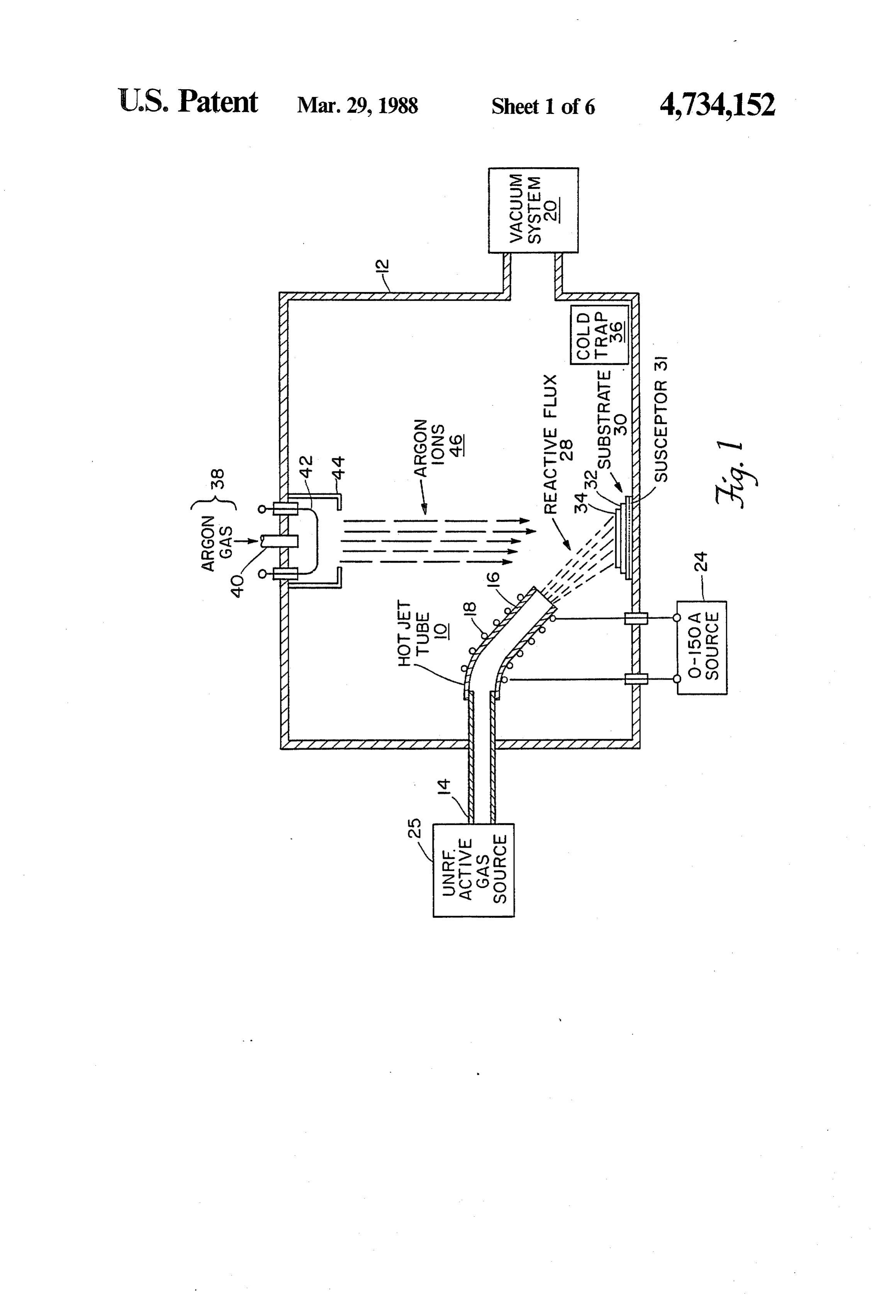
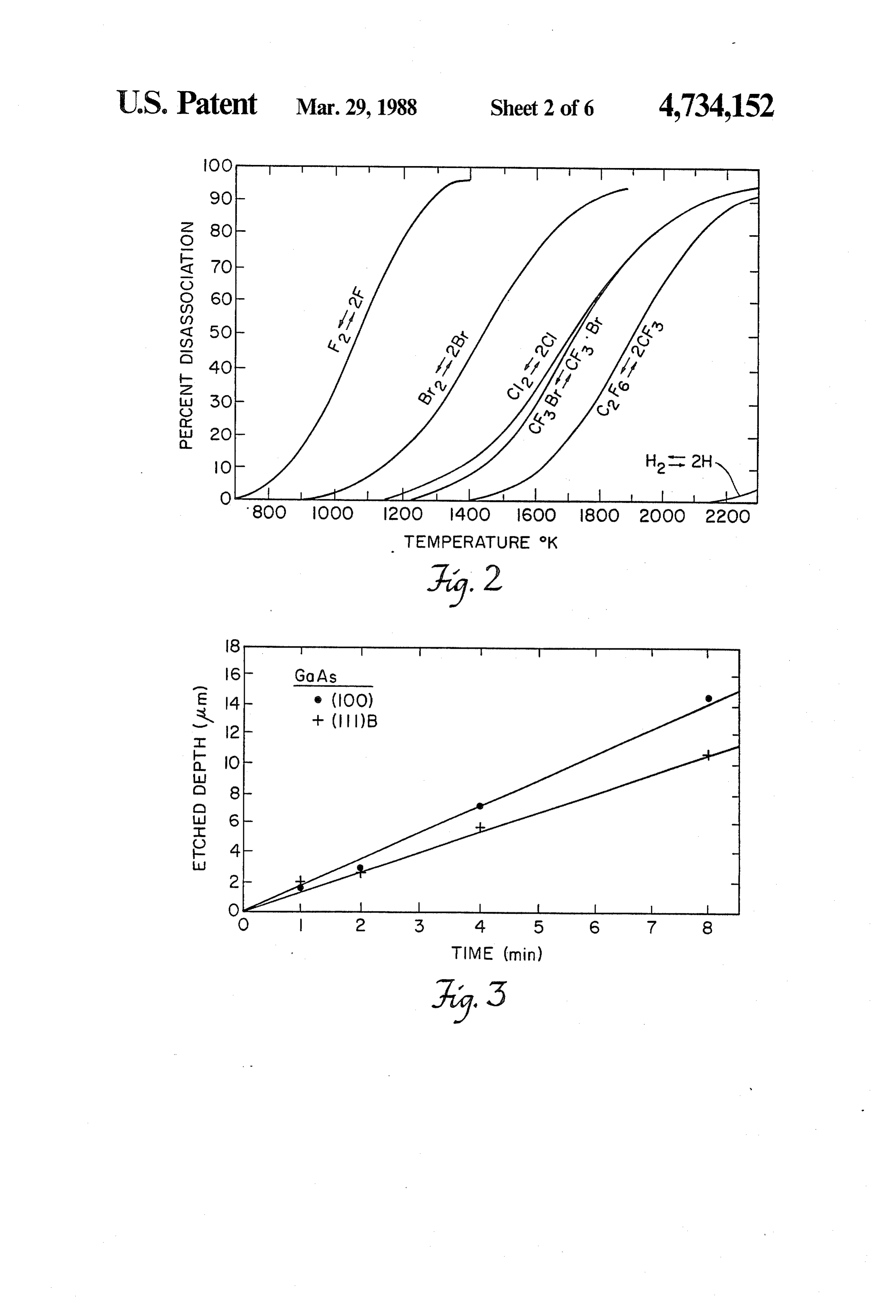
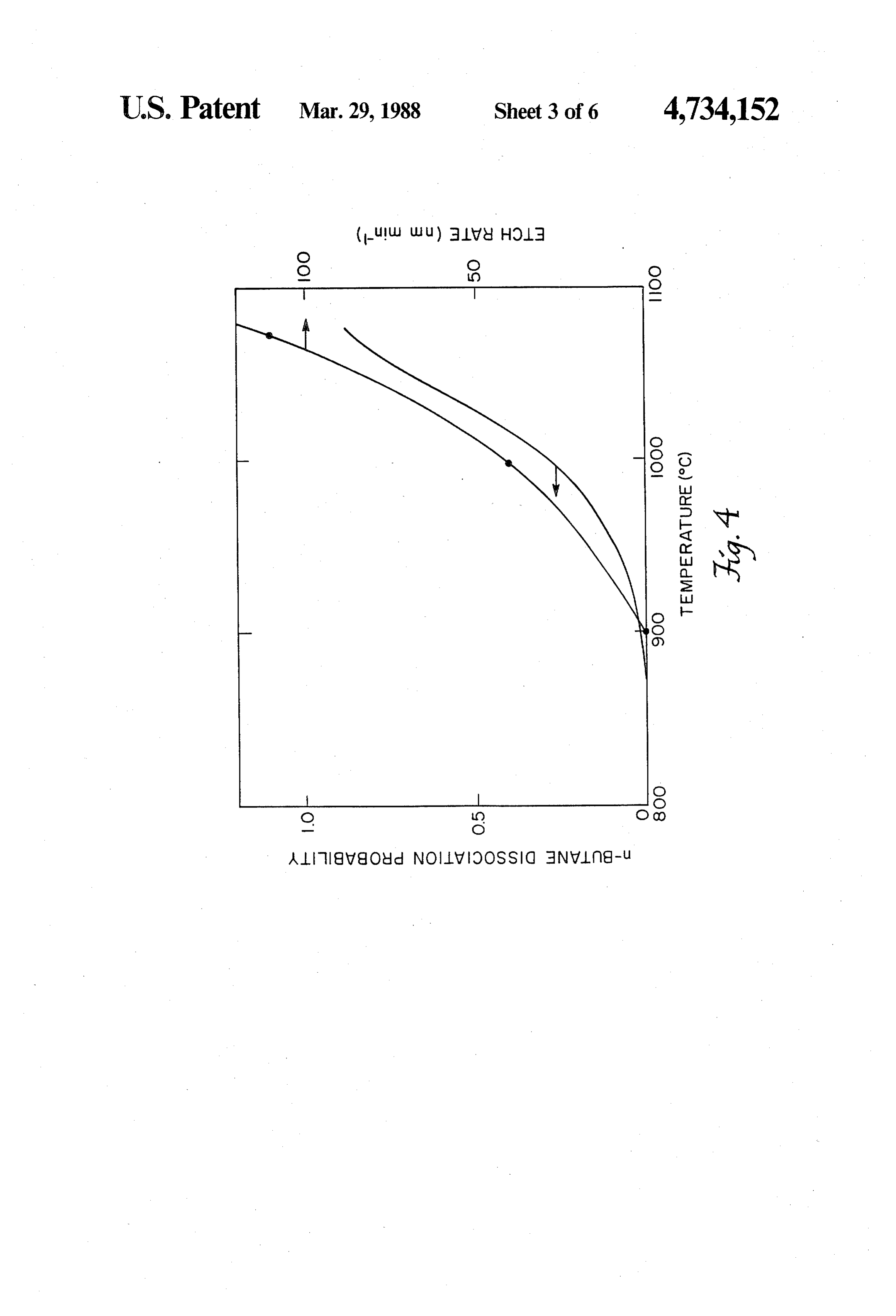
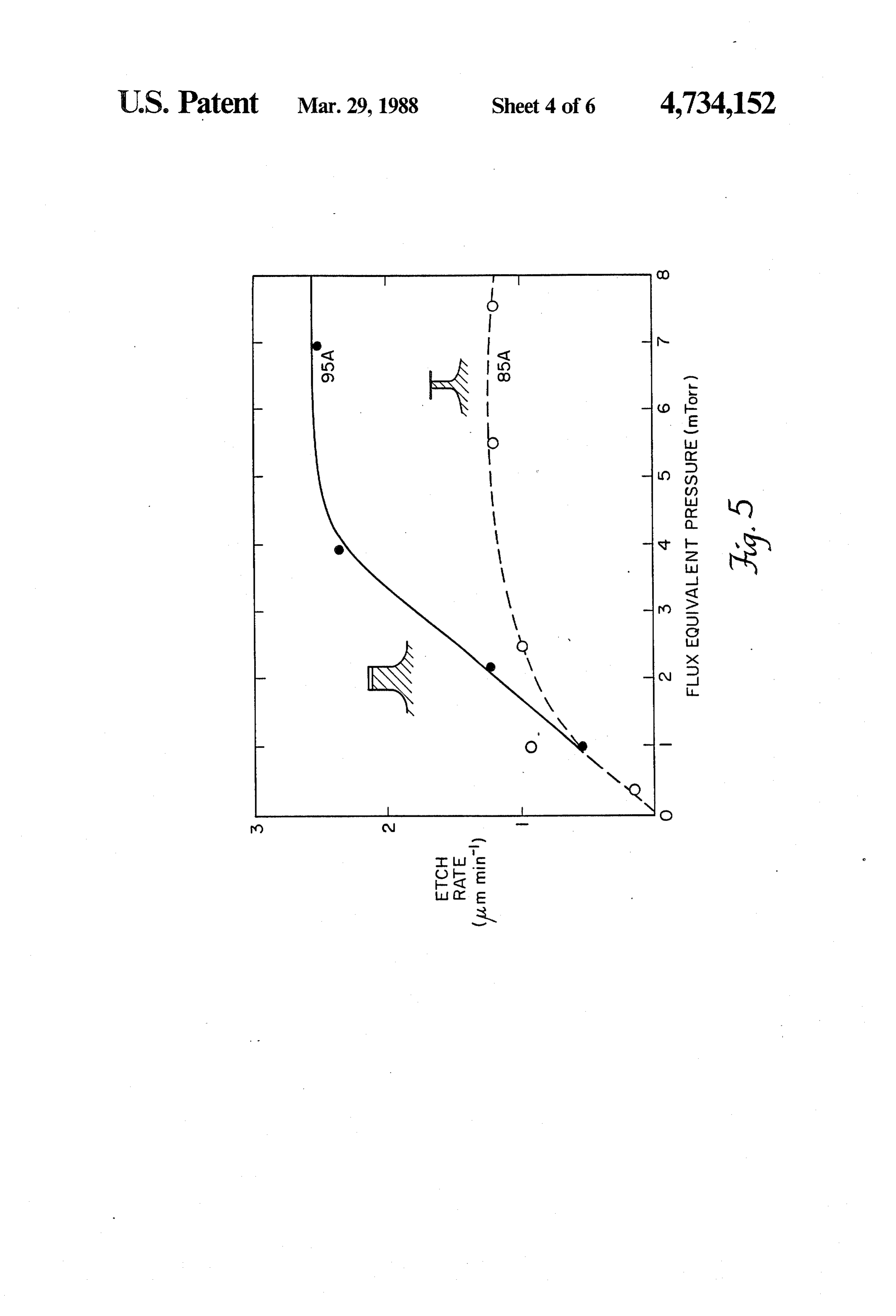
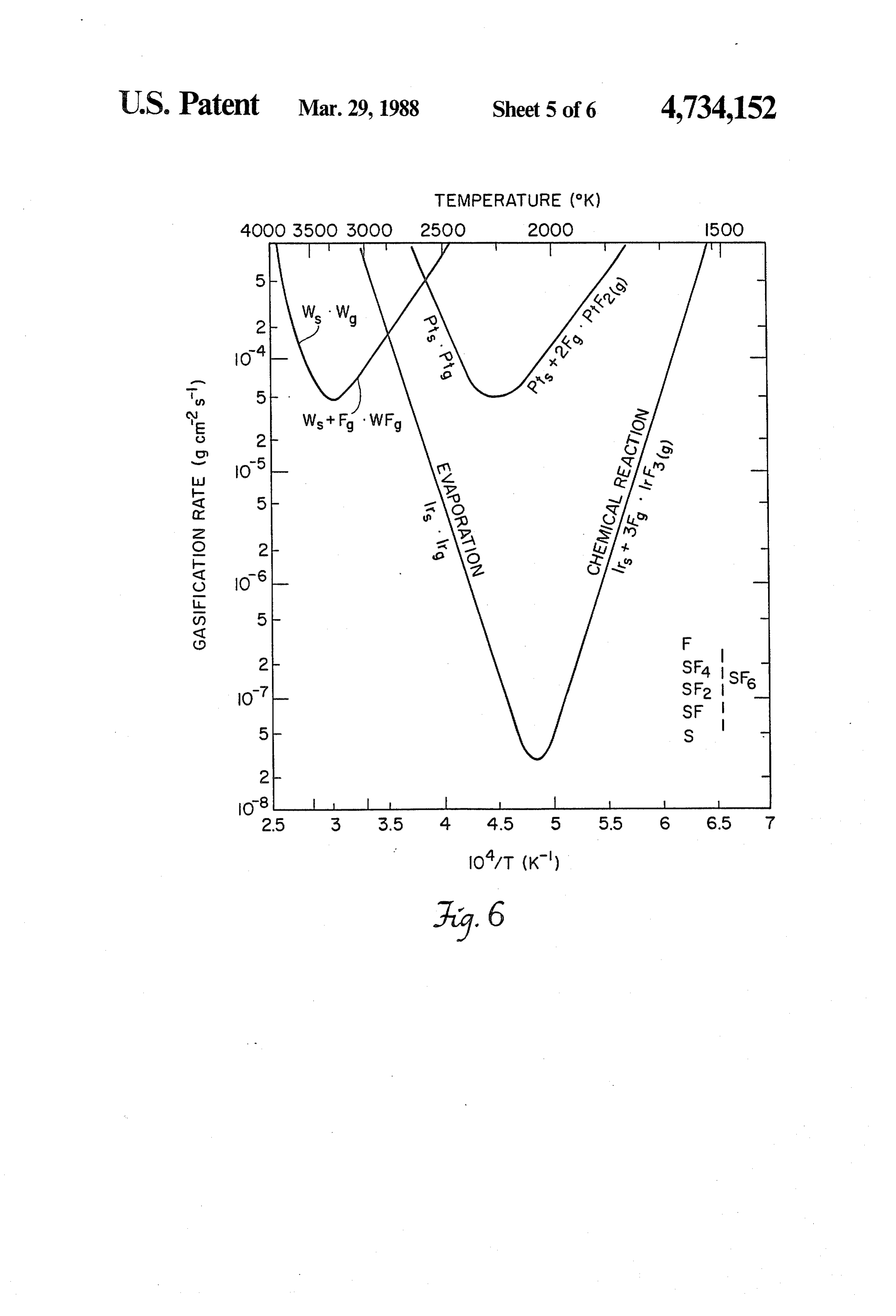
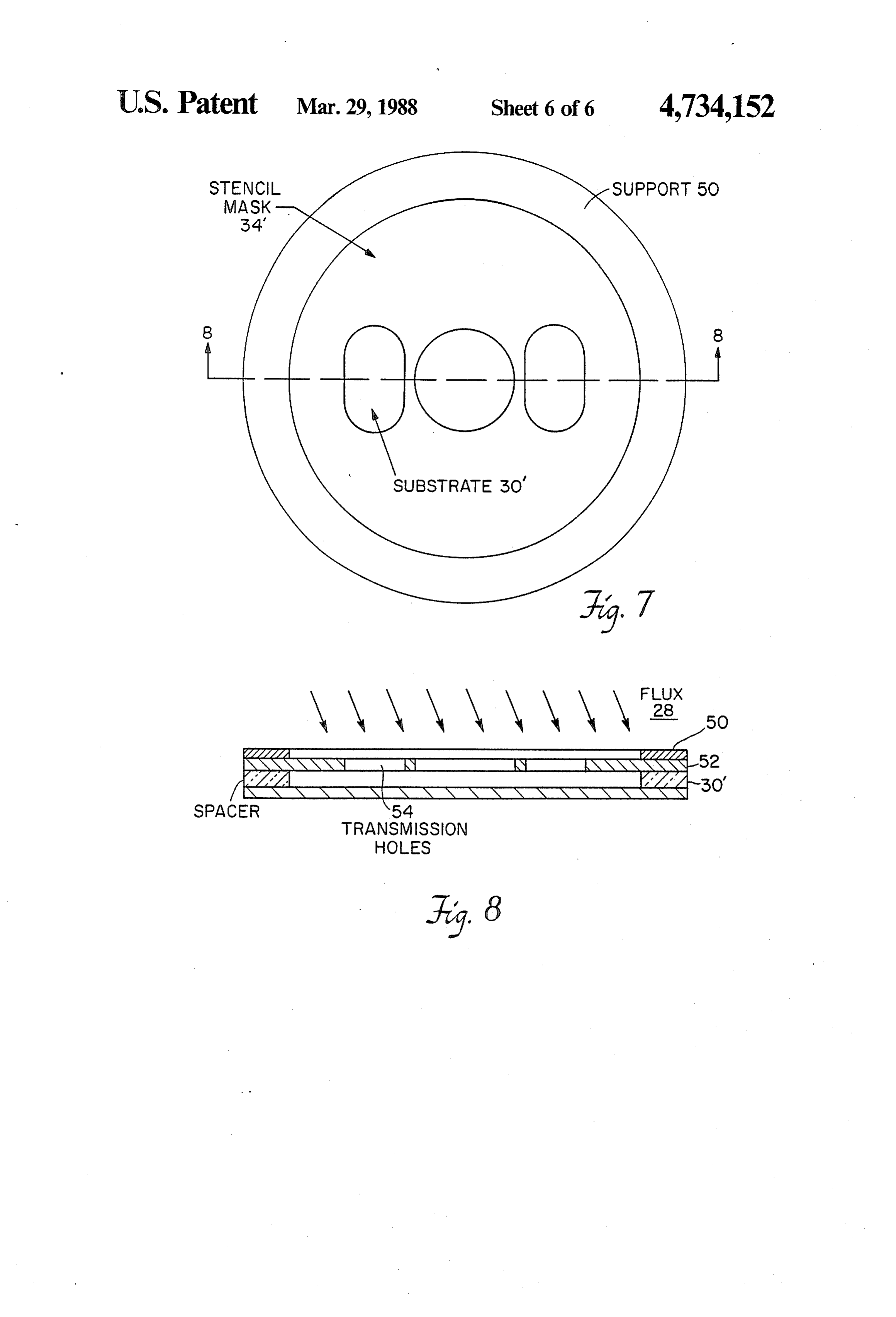
FIG. 6 is a plot of the gasification rate of tungsten decomposition.
FIG. 7 is a top planar view of the use of a reusable 20 heated to heated resistively tungsten tube was employed. It was temperatures between 1500 and 2000 C.
FIG. 8 is a cross-sectional view taken along lines 8-8 Chlorine was used as a feed gas. Chlorine is known to of FIG. 7. react with tungsten attemperatures above 300° C. form ing a variety of volatile tungsten chlorides. However, at
Page 2drawing sheetscan →
Page 3drawing sheetscan →
Page 4drawing sheetscan →
Page 5drawing sheetscan →
Page 6drawing sheetscan →
Page 7drawing sheetscan →
Page 8scan →
Conventional dry anisotropic etching, used for semi
DRY ETCHING PATTERNING OF ELECTRICAL conductor device fabrication, is accomplished by plac AND OPTICAL MATERLALS ing the material to be etched in a plasma. The plasma produces both ions and molecules with an incomplete
GOVERNMENT SPONSORSHIP bonding structure (radicals). The radicals are used to This invention was made in the course of work sup chemically react with the substrate forming volatile ported by the U.S. Air Force under Contract No. tion reaction products. The ions are used to initiate the reac F19628-85-C-0002. This is a continuation of co-pending flux between is the radicals and substrate. Since the ion directional, the etching is substantially aniso application Ser. No. 945,081, filed on Dec. 22, 1986, 10 tropic.
now abandoned.
While dry etching, as described above, is superior in
BACKGROUND ART many respects to wet etching, a number of disadvan In the manufacture of electronic or optoelectronic ample, tages are present in the conventional systems. For ex integrated circuits, an essential step is the patterning of 15 occurs. ion bombardment is non-selective. Sputtering Thus, in addition to etching the SiO2 material, a particular sequence of successive layers of insulative, the ion bombardment can etch adjacent resist material semiconductive, conductive or optical material on a substrate. A common example is the patterning of a andAlso, underlying Simaterial.
the ion beam can damage adjacent or underly silicon dioxide (SiO2) layer formed on an epitaxial sili ing material.
con substrate for the purpose of selectively removing and UV lightGate oxides can be damaged by electrons emissions. The ion beam equipment is the insulating layer to expose the underlying silicon. 20 relatively
Typically, a thin film of organic "resist” material is relatively expensive slow, i.e., and complex. The etching rates are less than 1 micron per minute. For formed over the SiO2 layer. these and other reasons, a need exists for an improved Next, a mask, comprising a transparent support mate anisotropic dry etching process.
rial coated with a thin layer of opaque material en 25 graved with the desired pattern, is placed on the resist DISCLOSURE OF THE INVENTION surface. The engraved openings in the mask are located where it is desired to removed SiO2 to expose the Si dryInetching accordance with the present invention, anisotropic is accomplished by directing a hot jet, or substrate.
flux, of a chemically
An intense beam of ionizing radiation from a source 30 thermal decomposition reactive species obtained from the of ultraviolet light, or laser energy or X-rays, is pro gasses. of comparatively unreactive More specifically, jected onto the back surface of the mask and breaks ing of source gasses in a tube the invention relates to heat down the molecular structure of the organic resist at alloy of tungsten and rhenium formed or of rhenium or an irridium to a tempera openings in the mask. The exposed resist material is ture in the range of about 900-3000 Kelvin dissolved by immersing the wafer in a suitable solvent. 35 pose such gasses and obtain a hotjet of reactivetoradicals. decom In this manner, the opaque mask geometry is transferred The irridium (Ir) jet tube is specifically used in con onto the resist material on the SiO2 surface. junction with a gas, such as SF6, containing fluorine to This resist pattern is now transferred to the SiO2, produce a hotjet of fluorine radicals for etching silicon itself, by exposing the wafer to a material that will etch through openings formed in SiO2.
SiO2 but will not attack either the organic resist material 40 The new dry etching system does not require either a or the Si substrate surface. This etching step is conven tionally accomplished with hydrofluoric acid, which plasma or ions. Radicals necessary for etching are ob tained by thermally decomposing an unreactive gas in a easily dissolves SiO2, but is incapable of etching or heated tube. The reactive radicals are directed from the dissolving the organic resist. Next, the remaining or heated tube on to material to be etched. The etching is ganic resist is removed by a suitable organic, or acid, 45 anisotropic by virtue of the directed flow and the fact solvent. that the radicals are selected to react chemically with The above process is a positive resist process in the material to be etched but not with adjacent or un which the resist material remaining after exposure and derlying material.
development, corresponds to the opaque mask areas. This system can be used to etch substrates very Negative resists are also in common use. 50 quickly. For example, silicon can be etched at a rate of The process in the above example, wherein the resist 3 micron/min with an anisotropic etching ratio (of the or SiO2 is etched away by an acid, is termed a wet etch depth to under cutting distance) of 5. Previously, etching process. Wet etching processes are difficult to the fastest etching rate for Si was in the range of 1 control because they lack sufficient anisotropic proper micron/min. In the present invention, at lower etching ties and, hence, result in an uncontrolled spread out of 55 rates (0.5 micron/min) the etching selectivity between the etching width. Therefore, as requirements for pat Si and SiO2 is approximately 1000 to 1, which is far in terning at the submicron level have developed, alterna excess of any other known dry etching system. tive anisotropic etching techniques have been devel This system may also be used to etch lead, Pb, which oped using "dry' processes. is an important material for superconducting devices. Anisotropic dry etching is usually accomplished with 60 Previously, no known system for dry etching Pb had a combination of ions and chemically reactive species been available. Etching of lead is accomplished by de produced in a plasma from an unreactive gas. The ions composing butane which forms CH3 radicals that react are accelerated out of the plasma onto the material with Pb.
exposed through the resist where they initiate chemical Etching may be accomplished through a reusable reactions between the reactive species and the material 65 stencil mask formed of material not chemically active forming volatile products. The directional nature of the with the reactive radicals of the hotjet. For example, in ion flux is responsible for the anisotropic character of etching Pb with CH3 radicals, a stencil mask formed of this etching technique. SiN, whereinx is in the range of 0.5 to 1.5 is preferred.
Page 9scan →
Brief description of the drawings
The fractional dissociation of non-reactive gasses into free radicals for anisotropic etching depends upon the
FIG. 1 is a schematic of the etching system of the gas temperature and pressure. The calculated percent invention. age of free radicals formed in a hotjet tube as a function FIG. 2 is a plot of percent dissociation versus temper 5 of temperature is shown in FIG. 2. For a number of ature in degrees Kelvin for various reactants. gasses, these calculations assume an estimated experi FIG. 3 is a plot of etched depth in microns versus mental room temperature pressure in the jet of 20 Torr. time in minutes for GaAs for two crystolographic Since the mass flow of gas is held constant in these planes o = (100) plane and + = (111) B plane. experiments, the gas pressure in the hot jet tube is as FIG. 4 is a plot of the dissociation rate of n-butane 10 sumed to increase with the square root of temperature and the observed lead etching rate as a function of ten and the percentage of gas dissociation. Gasses like F2, perature in degrees Centigrade. Br2, Cl2, CF3Br, and CF3CF3 can be easily decomposed FIG. 5 is a plot of etch rate in micron/minute versus chlorine flux equivalent pressure in miliTorr for two into free radicals at temperatures less than 1800 K. However, gasses like H2, N2, or CF4 require higher different jet temperatures related to two different heat 15 temperatures or lower gas pressures to obtain thermal ing currents, i.e., 95 amperes and 85 amperes.
FIG. 6 is a plot of the gasification rate of tungsten decomposition.
The stability of the hot jet tube depends upon the
(W), platinum (Pt) and irridium (Ir), as a function of material composition of the tube. In one experiment, a temperature.
FIG. 7 is a top planar view of the use of a reusable 20 heated to heated resistively tungsten tube was employed. It was temperatures between 1500 and 2000 C.
sterile mask in accordance with the invention.
FIG. 8 is a cross-sectional view taken along lines 8-8 Chlorine was used as a feed gas. Chlorine is known to of FIG. 7. react with tungsten attemperatures above 300° C. form ing a variety of volatile tungsten chlorides. However, at
BEST MODE OF CARRYING OUT THE 25 temperatures above 1500 C., tungsten becomes inert to INVENTION Cl2. This insures that the hot jet will operate with Cl2, Referring now to FIG. 1, the invention will now be contactprovided all the tungsten surfaces which will come in described, in detail, in connection therewith. The appa with Cl2 are above 1500 C. Hot jet tubes have ratus of the invention comprises, in general, a stainless been operated with Cl2 for up to an hour without degra steel vacuum chamber 12 within which a substrate or 30 dation. However, when these tubes are operated below wafer 30, having a film 32 formed thereon, may be 1500 C., the Cl2 will etch the tungsten tube away in less mounted on an air-cooled heat sink susceptor 31 for than 20 seconds. Gasses like CF3Br are comparatively etching. A reusable stencil or, alternatively, a resist 34 unreactive and the tube material is not critical. Other with patterned openings is placed or formed on the film gasses like SF6 are very reactive with hot tungsten and 32 to define the areas in the film to be etched. 35 although hot jet tubes have been operated with this gas Optionally, a Kaufman ion source 42 using Argon gas for tens of minutes, the tube will more commonly etch 38 may be used to generate Argon ions, or equivalent, away in a few seconds. Using the hotjet tube system of through a grid 44 to sputter clean the surface of the film the invention, a variety of materials have been etched, prior to etching. A resistively heated tube 10, in the as shown in Table 1, below:
form of a metallic tube 16, encircled by a heater coil 28 TABLE 1. is coupled to a current source 24. Alternatively, current Hot jet etching (units nm min) can be passed from one end of the tube to the other to Source Etched Material Thermal Photoresist heat it.
Unreactive gasses from source 25 are coupled Examples Gas GaAs Si SiO2 (Novoac) through an alumina, quartz or carbon tube 14 to the 45
CFBr interior of hotjet tube 10, where the unreactive gas or 3 SF6 <0.1 200-300 <0.1 <0.1 gasses are disassociated to form a directed flux 38 of hot *um min reactive species. A liquid nitrogen cold trap 36 is em ployed to pump both the unused reactive species and the reactive products. 50 These etching rates were obtained with a hotjet exit The vacuum system 20 may consist of a 4-inch liquid pressure estimated between 20 and 60 Torr, a sample nitrogen cold trapped diffusion pump with a base pres flux equivalent pressure between 3 and 10 mTorr, and a sure of 5x 10⁻⁷ Torr. hot jet temperature between 1000 and 3000 C. or Etching is accomplished by first sputter cleaning the Kelvin.
face surface of the substrate through exposed openings 55 Since there is no ion beam used during the etching of with Argon ions, after which the ion beam is turned off the samples, except to sputter clean the sample surface, and the reactive species 28, produced from the hot jet high differential etching rates are possible. This results tube 10, are allowed to etch the exposed surface of film from the fact that the ion beam etches, to some extent, 32 through the resist or stencil or oxide openings. everything the ions hit, whereas gas sources used herein The production of the reactive species depends upon 60 are selected to produce radicals which selectively etch the unreactive feed gas material in source 25, the tem only the desired material. For example, in the examples perature of the hot jet tube 10, and the chemical and given in Table 1, only the GaAs or Si is etched to any thermal stability of the hot jet tube. Theoretically, any substantial extent, while the SiO2 or resist remains sub gas consisting of two or more elements can be decom stantially intact. Thus, the etching rates of the photore posed at a sufficiently high temperature. However, 65 sist and SiO2 were too small to measure, i.e., 0.1 nm. because of tube material limitations, the hot jet tube min, when Cl2 was used as a feed gas. Even a few cannot be operated above or below certain temperature nanometers-thick native oxide on top of the GaAssam limits. ple is sufficient to mask the sample during etching.
Page 10scan →
Since there is no ion beam used during the etching, any accumulation of material on the etching surface (1) from the hot jet or the vacuum system may cause the CH3CH2CH2CH, heate 2 CH3CH, reduction of the etching rate. To check for this, the etch depth into GaAs was plotted as a function of the etch CH3CH2CH2CHs heate CH3+ CH3CH2CH, (2)2 ing time, as shown in FIG. 3. The etch depth is a linear function of the etching time, indicating that there is no Reactions (1) and (2) are believed to occur with equal evidence of contamination. Etched depths as deep as 75 probability. The dissociation probability of n-butane microns have been obtained without any indication of 10 and the observed Pb etching rate as a function of tem the etch rate diminishing. perature is shown in FIG. 4. The lead is believed to be The etch rate for Cl2 feed gas on GaAs was found to etched by the reaction be linearly dependent upon the equivalent flux pressure of reactive species on the sample, up to a pressure of 6 Pb(s)+4 CHR-Pb(CHR) (3) mTorr. Above 6 mTorr, the etching rate became nearly 5
COnStant. where R represents one of the radicals H, CH3, or The anisotropic nature of the etching technique was CH3CH2. Etching rates as high as 0.6 microns mini proven by a scanning electron micrograph of an etched have been obtained with a n-butane flux-equivalent GaAs sample. The etched depth is approximately 50 pressure of 1 mTorr. This is consistent with approxi microns with 10 microns of undercutting. An aniso 20 mately one-quarter of the maximum available radicals, tropic etch ratio of the etch depth to the undercutting which could beformed by reactions (1) and (2), reacting distance of 5, is acceptable for some device fabrication with the Pb film. Tin and several transition elements, and etched through holes in GaAs wafers. Etching such as Zn, Cd, Te, Hg, have been etched with these uniformity better than 10% was obtained over an area 4 methyl and ethyl radicals. So far, Ge, Si, GaAs, and InP cm in diameter. 25 have exhibited no measurable etching rates, using the In improved embodiments of the invention, the tung abovevolatile reactants, although these elements are known to sten hot jet tube was replaced by a tungsten/rhenium form cals.
compounds with methyl and ethyl radi alloy tube or an irridium or rhenium tube allowing much higher temperatures, i.e., up to 3000 C. to be EXAMPLE II: ETCHING GaAs attained, without noticeable tube degradation. 30
The hot jet etching system can also be used to etch
Lead, gallium arsenide and silicon may be etched, in GaAs through openings in a resist formed of post-baked accordance with the invention, as described in the foll Novolac-resin photoresist. In this process, chlorine is lowing examples: usually used to etch GaAs by the following reactions:
The Pb samples used in these etching examples con c HOT JET G2 CI (4)4. sisted of 0.5- to 3- micron thick, RF-sputter-deposited films of Pb on Si substrates. Standard photolithography 6 C1 + GaAs(s) - Gedacl: + AsCl3 was used to obtain 100-nm-thick resist patterns of No volac organic resin resist material on the Pb films. Etch ing was accomplished by first sputter-cleaning the Pb 6 C--GaAss)--GaCl3-i-AsCl3 (5) surface with a 0.1-mA cm-2 beam of 500-ev Ar-- ions for 1 min, which removes less than 10 nm of the Pb film. The effect shown in Table 1 was found to increase by After the cleaning, the source-gas flow is established at 45 replacing the tungsten jet with jets formed from an approximately 1 mTorr of flux-equivalent pressure on alloy of 20% rhenium and tungsten or a pure rhenium. the sample. Next, the jet tube, which is usually formed from tungsten foil, is heated to its operating tempera This increase in etching anisotropy may be the result of reduced contamination of the GaAs surface with the ture. Several source gasses, including n-butane (C4H10), marginally volatile tungsten chloride salts formed in the dimethyl ether ((CH3)2O), and acetone ((CH3)2CO), 50 jet. An etching anisotropy ratio of the etched depth to have been used, resulting in etch rates in excess of 100 the undercutting distance of approximately 10, has been nm min-1. obtained in GaAs using such a tungsten rhenium alloy Depending upon the etching conditions, after 0.5 to 1 jet.
microns of Pb is etched a protective film forms on the The etching rate and anisotropy were found to de sample which terminates the etching. Sputter cleaning, 55 pend upon both the jet temperature and the Cl2 pres using ion source 42, may be used to remove this film and sure, as shown in FIG. 5. Note: An estimated average allow hot-jet etching of the Pb until the protective film residence time of a molecule in the hotjet, which is used reforms. By using this system of alternate hot-jet etch to calculate the dissociation probability, was obtained ing and sputter cleaning, nearly vertically etched struc by dividing the length of the hot jet by the average tures can be obtained. A 3-um-thick Pb film was etched 60 molecular velocity. The estimated average residence completely through by 12 iterations of a 30-s sputter time at 1000 C. is 58 usec. Since it is difficult to charac cleaning and a 1-min hot-jet etching with dimethyl terize the actual internal jet temperature, the current ether. The sputtering alone etches approximately 100 used to heat the jet is used as a general indication of the nm of the Pb film. jet temperature. At the lower current, 85A, the result The source gas, n-butane, is believed to decompose at 65 ing temperature is estimated to be 2600 K, by equating jet temperatures in excess of 900' C. into methyl (CH3), the resistively dissipated power in the jet to power loss ethyl (CH3CH2), and propyl (CH3CH2CH2) radicals by by radiation. The etching rate saturates at about 1 the reactions: mTorr rf flux equivalent pressure of Cl2. At the higher 11 current, 95A, the temperature is estimated to be 2800 comprise SiN membranes 52 supported on Si sub K. and the etching rate saturates at approximately 4 strates, with transmission holes 54 lithographically mTorr of flux-equivalent pressure. In the saturated formed therein to define a pattern to be etched in a etching rate region, the etched structures had low etch substrate 30'. Submicrometer features for different de ing anisotropy ratios of about 2 for a current of 85A at vices have been defined in these stencil masks. a flux equivalent pressure of 7.5 mTorr. Etched struc Conventional procedures for pattern definition in tures exhibited etching anisotropy ratios of about 10, volve a lithography step, a wet chemical development when etched with a jet current of 95A and at pressures step, and an etching step. However, using hot jet etch below 4 mTorr.
It is believed that the efficiency of dissociation of the 10 ing with stencil masks, it is possible to eliminate the lithography and development steps. The stencil masks
Cl2 molecules, which determines the etching rate, de are placed directly over the substrates 30', with or with creases with the increase in Cl2 pressure and increases with an increase in temperature. At low Cl2 pressures or out a spacer in-between, and the patterns on the stencil masks are then transferred directly to the material un high heater currents, the majority of the reactive flux is derneath by hot jet etching using a flux 28 of suitable in the form of Cl and the etching rate increases with 15 reactant radicals. A potential problem for using stencil pressure. At higher pressures or lower jet temperatures, masks in combination with other dry etching techniques Cl2 dissociation is less and the etching remains constant with an increase in pressure. Under low pressure and is damage to the stencil masks due to ion bombardment.
high temperature conditions approximately 50% of the Since hotjet etching does not employ ion bombardment maximum available chlorine flux reacts with the sample. 20 on the materials, the high differential etching rates allow stencil masks to be used repeatedly for etching. In
EXAMPLE III: ETCHING SILICON accordance with the above-described invention, GaAs Silicon may be etched through openings in SiO2 or samples were etched through SiN. stencil masks with silicon nitride with a fluorine flux obtained from the feature sizes below 100 nm. thermal decomposition of a source gas of SF6, Since F 25 Hot jet etching with stencil masks is a new pattern is extremely reactive, the jet tube material is critical. At definition technique which allows lithography steps and low temperatures (<3000 K), Freacts with the tung wet chemical development steps to be eliminated which sten jet tube to form a variety of tungsten salts and the will, in turn, provide higher yield and throughput for jet tube, itself, is etched away. At higher temperatures device fabrication.
i (>3000 K.), these salts will decompose into W and F 30 Equivalents and the tungsten jet tube will become less reactive.
However, at still higher temperatures (>3500 K.), the While preferred embodiments have been shown and W will evaporate and the jet tube will fail in a short described above, various other equivalent embodiments time. FIG. 6 shows the gasification rate of W, Pt, and Ir and modifications will become apparent to those skilled as a function of temperature. The optimum operating 35 in the art based upon the description provided herein.
temperature for etching Si with a tungsten jet is be For example, in addition to the source gasses previously tween 3000 and 3500 K. However, even at these tem described, the following is a list of equivalent gasses and peratures, there is substantial loss of tungsten metal. radicals produced:
Consequently, one is only able to operate for as long as 40 minutes before the tungsten jet tube fails. Platinum is 40 more inert than tungsten, but its higher evaporation rate Gas Radical makes it unsuitable for jet tube material, because the Pb(CH3)4 CH3 evaporated Pt masks the sample and stops the etching. NF
We have found that Iris the optimum material for the CCl4 C jet tube. In practice, Irjet tubes have operated for sev 45 SiCl4 C eral hours without any sign of deterioration, provided they are operated between 1750 and 2500 K. How ever, Irjets do not provide as high etching rates as Also, the following significant integrated circuit or similar jets formed from W. optoelectronic etchable materials are listed, together Table 2, below, summarizes the etching rates for a with suggested suitable reactant flux radicals or mole variety of materials using several sources gasses. Note 50 cules for anisotropic etching thereof:
that the differential etching rate between SiO2 and Si is in excess of 1 in 1000. Material To Be Etched Radical/or Molecule TABLE 2 GaAs Cl
SOURCE 55 Si Cl or F GAS GaAs Si SiO2 Pb PH Alu IP Cl and CH3 Cl 1 x 10 O <0.1 CO. <1 HgCdTe, Se CH3
SF6 2 x 10 <2 <2 InGaAs Cl and CH3" C4H10 <5 6 x 10² <2 <2 W F Hot-jet etching rates (nm min) of a variety of commonly used materials for 60 WSi F several source gasses. The jet-to-sample distance in these Examples is approximately SiO2 H 10 cm with the exception of the etching rate neasurements made with GaAs, for SiN F which the jet-to-sample distance was approximately 4 cm. (100)-cut, n-type GaAs Ge, Sn, Si, As H and Sisamples were used to determine the etching rates. SiO2 films were obtained by thermal oxidation of Si wafers, and PH is a Novolac-resin photoresists. Organic Photoresist O *Note: In this case, more than one radical is required to etch different materials,
Hot Jet Etching with Stencil Masks This completes the description of the preferred em Details of the stencil mask embodiment of the inven bodiments of the invention. Since numerous modifica tion are shown in FIGS. 7 and 8. The stencil masks 34 tions and changes will occur to those skilled in the art, 12 it is not intended that the invention be limited to the which is coupled to said source of feed gas; and exact construction and operation shown and described wherein said tube is formed of a metal from the herein. Accordingly, all suitable modifications and group comprising irridium or rhenium or an alloy equivalents are intended to fall within the scope of the thereof.
following claims. 5 11. The apparatus of claim 10 wherein the tube is We claim: adapted to be resistively heated by an encircling wire 1. Apparatus for etching a first material through coil through which current is passed. openings formed in a mask, comprising: 12. The apparatus of claim 10 wherein the source gas (a) a source offeed gas containing species which are is taken from the group comprising: hydrogen, fluorine, chemically reactive with respect to said first mate 10 chlorine, bromine, methane and ethane. rial when dissociated from said gas by heating; 13. The apparatus of claim 10 wherein the source gas (b) a reusable stencil mask over said first material and is chlorine, the first material is GaAs and the second formed of a second material which is not chemi material is a photoresist.
cally reactive with respect to said species; 14. The apparatus of claim 10 wherein the source gas (c) heater means for heating said feed gas to a temper 15 is fluorine or a compound containing fluorine, and the ature which dissociates said gas and forms species first material is silicon while the second material is SiO2; of said gas which react with said first material to and the temperature is between about 1750 and 3300 etch said first material without substantially etch K.
ing said second material. 15. The apparatus of claim 10 wherein the source gas 2. The apparatus of claim 1 wherein the heater means is taken comprises a heatable hollow tube having a proximal and dimethylfrom the group comprising n-butane, Pb(CH3)4, ether or acetone and the first material is lead distal end, the distal end of which is directed at the openings and the proximal end of which is coupled to while the second material is a photoresist. 16. The apparatus of claim 10 wherein the source gas said source of feed gas. contains fluorine and the first material is tungsten or 3. The apparatus of claim 2 wherein the tube is 25 silicon nitride.
formed of rhenium.
4. The apparatus of claim 2 wherein the tube is contains hydrogen The apparatus of claim 10 wherein the source gas formed of irridium. and the first material is SiO2, Ge, Sn, 5. The apparatus of claim 2 wherein the tube is Si or As.
adapted to be resistively heated to a temperature in a 30 18. The apparatus of claim 10 wherein the source gas range of 900 to 3000 degrees Kelvin. contains Cl and CH3 radicals and the first material is InP 6. The apparatus of claim 1 wherein the source gas is or InCaAs.
taken from the group comprising hydrogen, fluorine, 19. The apparatus of claim 10 wherein the source gas chlorine, bromine, methane and ethane. contains CH3 radicals and the first material is HgCdTe 7. The apparatus of claim 2 wherein the tube is 35 or Pb, Zn, Sn, As, Se, Cd or Te.
formed of metal from the group comprising rhenium 20. The apparatus of claim 10 wherein the source gas and irridium, or an alloy thereof, the source gas is chlo contains Cl radicals and the first material is from the rine, the first material is GaAs and the second material group comprising Si, AlGaAs, and GaAs. is SiN. wherein x is in the range of 1.5 to 0.5. 21. The apparatus of claim 10 wherein the source gas 8. The apparatus of claim 2 wherein the tube is contains H radicals and the first material is from the formed of irridium, the source gas is fluorine or a com group comprising Ge, Sn, Si, As, SiO2. pound containing fluorine, and the first material is sili 22. The apparatus of claim 10 wherein the source gas con; and the temperature is between about 1750 and contains oxygen radicals and the first material is from 2SOO. K. the group comprising organic photoresist. 9. The apparatus of claim 2 wherein the source gas is 45 23. A method for anisotropic etching of substrate taken from the group comprising n-butane, dimethyl material through openings formed in a mask comprising ether or acetone and the first material is lead. the steps of:
10. Apparatus for etching a first material through (a) providing a source of gas containing radicals openings formed in a second material, comprising: which, when heated, dissociate said radicals being (a) a source of feed gas containing radicals which, 50 capable of volatilizing said substrate material but when separated by thermal energy, are chemically not said mask material;
reactive with said first material and chemically (b) heating said gas to dissociate said radicals and unreactive with said second material; directing said heated gas toward said openings to (b) heater means for heating said gas to a temperature volatilize said material using a rhenium or irridium which dissociates said gas and forms said radicals 55 hot metal tube having a proximal end coupled to of said gas which react with said first material to said gas source and an open distal end facing said etch said first material without substantially etch openings.
ing said second material; and wherein the heater 24. The method of claim 23 wherein the mask is a means comprises a hollow heatable tube having a reusable stencil formed of SiN. where 'x' is in the distal and proximal end, the distal end of which is 60 range of about 1.5 to 0.5.
directed at the openings and the proximal end of a k c s
Provenance
- Collection
- Patents citing this work
- Pages
- 12
- Method
- pdftotext (the PDF's own text layer) + pdftoppm 300dpi page scans
- Patent office record
- patents.google.com →
- Source
- Google Patents citing-documents table
- Assignee
- Massachusetts Institute Of Technology
- Published
- 1988-03-29
- Transcribed from
- patentimages.storage.googleapis.com →