Step Charge as a function of Pulse Period
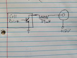
Here we can see the Cell Driver Circuit pulsing a double cell in parallel. The arrangement is powered by a 12V ATX supply. The Cell Driver's inputs: Vcc and Vee are both B+ 12VDC REG.
This inductor appears to be playing the role of Vc2. When I introduce a mutually coupled Vc1 (the other side of the core at 612mH), regardless of phase, all modulation and/or rise is completely dampened.
Too large of an inductance at the Vc2 position (in this specific arrangement), dampens out all modulation.
Too small of an inductance at the Vc2 position (etc), allows much more of the pulse to be reproduced at the load Vout, and "Cell Saturation" is perhaps reached too soon.
Too large of an inductance in a Vc1 position also significantly inhibits modulation, unless sufficient offsetting capacitance is added in the form of parasitics, distributed coupling or external parallel capacitance.
Perhaps this is the reason for the inverted pulse trains feeding the Cell Driver input. If a constant DC bias during "offtime" is applied, then during the pulse pull down, inductive reversal directed by the diode, is responsible for the higher voltage spikes.
This process cumulatively increases the bias of the cell cathode with each successive pulse. The voltage will rise (return) up to at least the available source voltage, or higher with the spikes. Given a higher voltage input, it seems quite possible that the 8XA style variac power supply, with added filtering, could supply the load directly (replacing the 12V REG here), up to 60VDC at least regarding the TIP120 thresholds (100V TIP122). Utilizing a higher voltage input would presumably result in much higher amplitude spikes, with the same 2.5V threshold, which appears to be the forward voltage drop across the TIP Collector/Emitter junction.
Schematic for arrangement
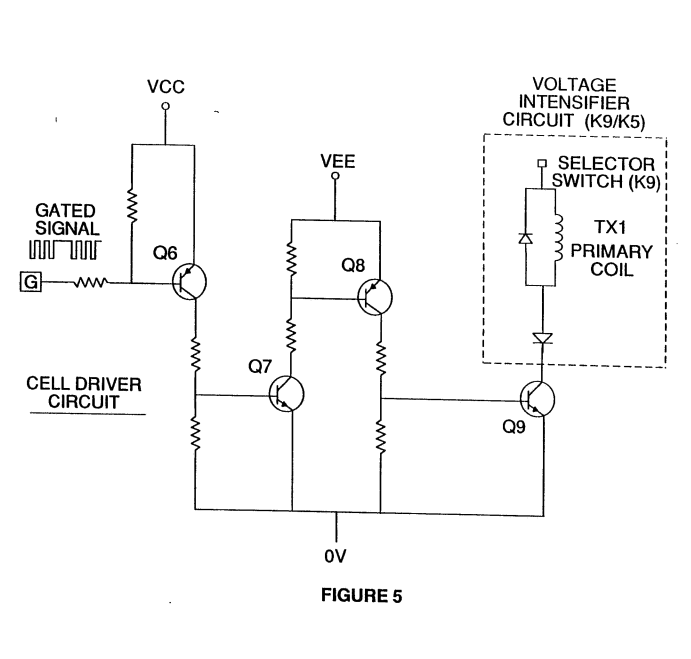
Cell Driver Circuit