
ENERGY of the FUTURE - R&Z - Vol 2 No. 3, 1991
ENERGY of the FUTURE
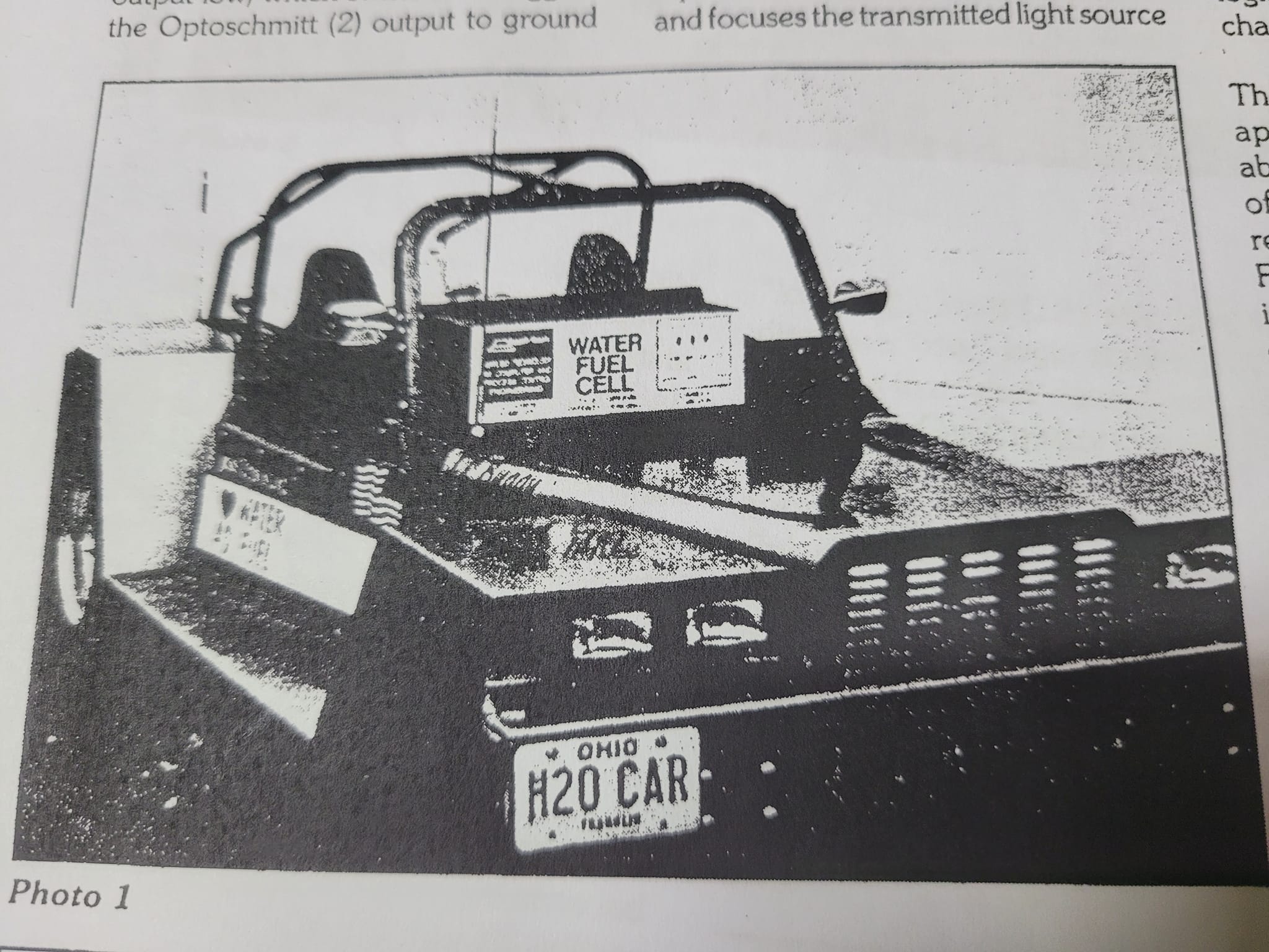
WATER FUEL CELL Copyright © 1990 by Stanley A. Meyer - Rahm & Zeit
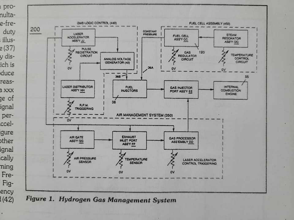
WFC Hydrogen Gas Management System - Part I
The WFC Hydrogen Gas Management System encompasses many processing patents into a full system-engineering approach to help give a viable answer to the energy problem...by using "Water" as a new Fuel-Source.
The WFC Hydrogen Gas Management (GMS) System not only economically produces "Hydrogen-Fuel" on demand from water but, also, renders Hydrogen-Fuel safer than natural gas allowing existing cars, trucks, or even jets to run on or be powered by Water.
The WFC Hydrogen Gas management (GMS) System is systematically activated and performed in the following way as a retrofit energy-system...defining "Mode of Operability"...on how to use "Water" Fuel.
Related Patents: 4,265,224, 1,213,671, 4,465,455, 4,798,661, 4,826,581, 4,613,304, 1,235,669, 4,275,950 , 1,234,774, 3,970,070 , 1,234,773
WFC Hydrogen Gas Management (GMS) System
Notice Of Technology All rights reserved. Printed in the United States of America. Except in the case of brief quotations embodied in critical articles or review, no part of this WFC tech-brief may be reproduced in any form or by any means, or stored in a databank or retrieval system without express written permission of inventor Stanley A. Meyer. For written approval, fax (614) 871-8075 or send request to 3792 Broadway, Grove City, Ohio 43123.
All graphic illustrations were created and registered under international UCC copyright laws by Stanley A. Meyer.
National Security Laws Patent security is enforced by National Security Laws of each participating country. Do "not" make, sell, or utilize a patented process and/or device without inventor written consent and approval. International patent and copyright laws mandate the same "usage" restrictions.Foreign Grant License Notice: U.S. Government has allowed the WFC technology to go forward into the interna- tional market place by granting foreign grant license No. 492680 issued July 10,1989 and foreign grant license No. 490606 issued Nov. 15, 1989 to Stanley A. Meyer as so specified and required under the Patent Cooperation Treaty (PCT) Act. Both U.S. & Foreign patents laws impose heavy fines & imprisonment on anyone who falsely claims to have participated in the development of any invention. Under the PCT Treaty Act, a declaration of Oath must be signed, certified, and registered prior to the filing of any PCT patent. Add after section titled "National Security Laws."
Illustrations
 |
 |
 |
 |
 |
 |
 |
 |
 |
 |
 |
 |
 |
 |
 |
 |
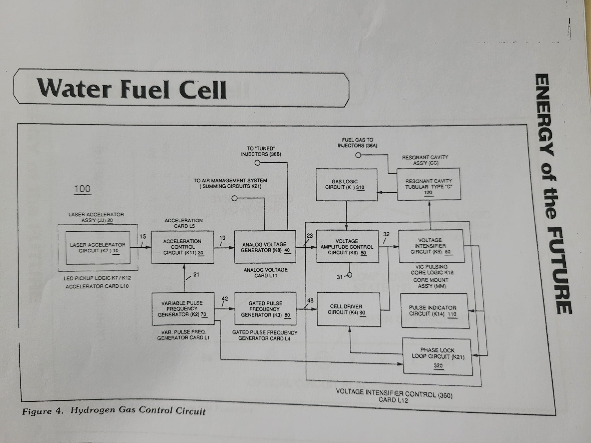
Water Fuel Cell
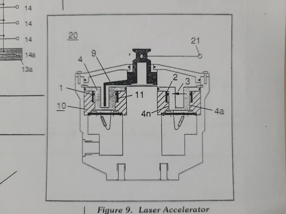
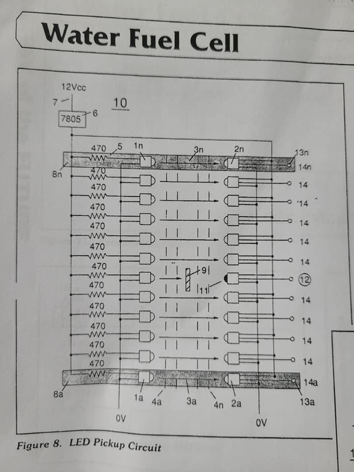
(4) which is a component part of Laser Accelerator Assembly (20) of Figure (9kses a GaAs infrared emitting diode (of figure (8) to trigger a SDP8611 Optoschmitt light receiver (2) of Figure (S) from quiescent state (output logic high. B-) (13) to on-state (the mini- mum irradiance that will switch the output low) which switches or triggers the Optoschmitt (2) output to ground state (zero (12). The peak wave- length (3) of Figure (8) being transmit- ted from the infrared emitting diode (ed) (1) to the Optoschmitt receiver (2) is typically (935 nm) and allows the Optoschmitt (2) clock frequency (the speed by which the Optoschmitt changes logic state) to be (100 khz). Optical lens (4) of Figure (9) redirects and focuses the transmitted light source
|
 |
(3) of Figure (8) (traveling infrared light waves) to the Optoschmitt (2) by pass- ing the light source through a series of concentric lenses (40 xxx 4n) of Figure (9) which become progressively smaller from the outer peripheral lens surface (4a) to the inner lens surface (4n). The spatially concentric lenses (4a xox 4n) of Figure (9) causes the beam angle of the light source to trigger the Optoschmitt (2) beyond the minimum irradiance that is needed to switch the Optoschmitt from quiescent state (high logic state/B+) to on-state (output changing to zero volts).
The Derate linearly of light intensity is approximately 125mW/degree C above 25 degree C at a spatial distance of 500 inches between the two infra- red devices (1X2) of Figure (8) as to Figure (9). Transmitted light source (3) is turned-on when an electrical power source of 5 volts is applied to the led () through dropping resister (5) by way of voltage regulator (6) connected to the car electrical system (7). Together, the matched infrared devices (1X2) with optical lens (4) forms optical circuit (8) of Figure (8). Grouping additional opt- cal circuits (8a xxxx 8n) in an in-line or linear arrangement, now, forms Led Pickup Circuit (10) of Figure (8), as shown in Figure assembly (20) of Fig- ure (9).
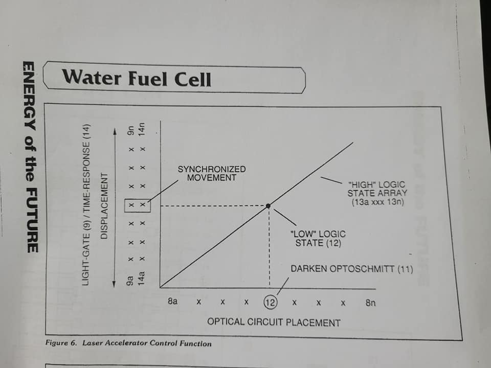
To perform a switch-logic function, light-gate (9) of Figure (8) as to Figure (9) is inserted between the matched infrared devices (1X2) and moved in a linear displacement from one optical circuit (8x) to another optical circuit (8xx), as illustrated in Figure (8)(9) as to Figure (6). Once light-gate (9) blocks and prevents traveling light-bear (3) from reaching the matched Optoschmitt (8xx), the darken Optoschmitt (11) (non-energized) changes output state since the irradiance energy level (3) isreduced to, or below the release point...triggering opposite logic state (12). As light-gate (9) advances to the next optical circuit (8xxx) a new and separate low-state logic function (12) occurs while the previous optical circuit (8xx) reverts back to high-state logic (13). Advancing light-gate (9) still further performs the same opposite (alternate) logic-state switching in a sequential manner until the advancing light-gate (9) reaches the last optical circuit (8) Reversing the movement of light gate (9) performs the same high to low logic witch function but in reverse sequential order. Reversing the direction of the light gate (?) once again reinstates the original sequential switching order, as illustrated in Figure (6) and Figure
Longevity and reliability of component life is typically 100,000 hours since led pickup circuit (10) of figure (8) utilizes no mechanical contacts to perform the sequential logic switch function. Light gate (9) integrated with led pickup circuit (10) make up Laser Accelerator assembly (20), as shown in Figure (9) Light-gate (9) of Figure (9) is mechanically linked to the car acceleration pedal by way of cabling hookup (22)
Opposite placement of the matched infrared devices (1)(2) prevents bogus or false triggering of "low" logic state (12) during light-gate displacement (9a xxx 9n) of Figure (6)(7) and (8). If light emitting diodes (led) (la xxxx ln) of figure (8) are electrically disconnected from DC power supply (6), then Led Pickup Circuit (10) outputs are switched to "low" logic state (12a xxxx 12n) which disallows "low" logic state signal (12), resulting in a "shut-down" condition to Hydrogen Gas Control Circuit (200) of Figure (1) Disconnection of power supply (6) to Optoschmitt array (2a ox 2n) of Figure (8) results in a similar "shut down" condition to control cir cult (200), as further shown in Figure (1). This "shut-down" or "Switch-off" condition helps provide a fail-safe operable Fuel Cell (120) of Figure (19) by negating acceleration beyond driver's control.
Acceleration Control Circuit (30)
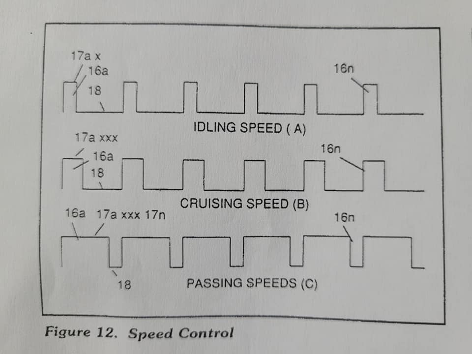
Moving light gate (9) of figure (8) in direct relationship to the physical placement of optical circuits (8a xxx 8n), sets up a time variable (14a xxx 14n) of Figure (6) from optical circuits (8x) to another optical circuit (8xxx) and/or (8xxxx) or to (8n) since the triggered low logic state (12) of Figure (6) and (7) moves in direct relationship to the displaced light-gate (9), as illustrated in Figure (11). Deflecting (moving) the light-gate (9) to position (8n) takes longer in response-time (14) than deflecting the light-gate to position (8x) and/or (8xx) or (8xxxx). This variable response-time (14axx...12...xx14n) or signal output (15) is now electrically transmitted to Acceleration Control Circuit (30) of Figure 4 since Laser Accelerator Assembly (20) of figure (9) converts mechanical deplacement (9a xx 9n) to electrical time-response (14a xxx 14n) of Figure (6) by linearly moving (forward and/or reverse direction) "low" logic state signal (12) in an array of "high" logic state output signals (13a xxx 13n), as further illustrated in Figure (7) and Figure (11). In some case reverse signal-logic (12axxx...13...xx12n) is applicable by using SDP8601 Optoschmitt which switches logic state from Quiescent static (low" to "high" logic state when de-energized.
Since Led Pickup Circuit (10) of Figure (8) operates up to 100 Khz range or above, electrical sensitivity of Opto-circuit (8) provides an instantaneous response to Driver's acceleration, de-acceleration, or cruise control demands.
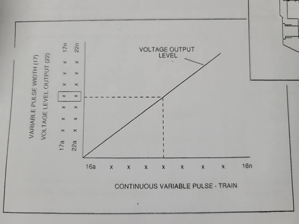
As signal output (15) of figure (4) (14 xxxx1214n) is being received by acceleration control circuit (30) of Figure (4) as to Figure (11), circuit (30) converts incoming timeresponse signal (140 x 12 x140) into a vari able time-base unipolar pulse (16), as shown in Figure (7) Circuit (30) electronically and automatically scans out put signal-array (14axxx 12 xx14) (15) until circuit (30) locates, momentarily registers, and translates response- time (14a oxx... 12) into a variable unipolar pulse (17/18) of Figure (7) The sweeping action of the scanning circuit (30) always starts from position (9a) and moves point (8ax) to point (8axxx) of Figure (8)(11) until logic-point (12) is detected. Once logic signal (12) is detected, the sweeping action toggles and recycles back to start position (9a). This toggling (flip back) action elec tronically determines variable time-response (14a xxx) regardless of wherever logic point (12) is being momentarily displaced within circuit array (13a xxx 13n). Toggling action at full-scale deflection (13a xxxx 13n) occurs in the range of (10) Khz or above and thus, allows instant response to Driver's acceleration demands.
Toggling-time (scanning-time) is directly synchronized to light-gate (9) displacement which, in turn, circuit (30) further sets up and establishes a given pulse shape (16) of Figure (7). Circuit (30) continues to increase pulse width (170) of Figure (7) as the moni- tored (detected by scanning) toggling-time (14a xxxxx.12) Increases when toggle-point (12) moves farther away from start-position (9a) to stop-position (9n), as further shown in Figure 12 as to Figure (11). Pulse width (17a xxx 17n) diminishes when logic-point (12) reverses direction to start position (9a). Finally, circuit (30) reproduces the variable controlled tube-shape (16) in a continuous repetitive manner (16a xxxx 16n) of Fig- ure (12) and electrically transmits the resultant pulse-train signal (19) to Ana- log Voltage Circuit (40), as shown in Figure (4).
In retrospect to engine performance (gas pedal attenuation) (21) of Figure 19), a wider pulse width (17a xxx) of Figure (120) increases (accelerates) engine R.P.M.; whereas, smaller pulse-width (17ax) reduces ide accelerates) engine R.P.M. Cruising speed (128) of Figure (12) is simply accomplished when pulse width re- mains constant
Incoming clock pulse (21a xxx 21n) of Figure (15) originating from Pulse Fre quency Generator (70) of Figure (4) sets up the scan rate (toggling) by which signal input (15) of Figure (4) is elec tronically scanned by circuit (30). The resultant clock pulse (21) of Figure (15) as to Figure (4) is always adjusted to exceed driver's response time to allow for instant acceleration control
Analog Voltage Generator (40)
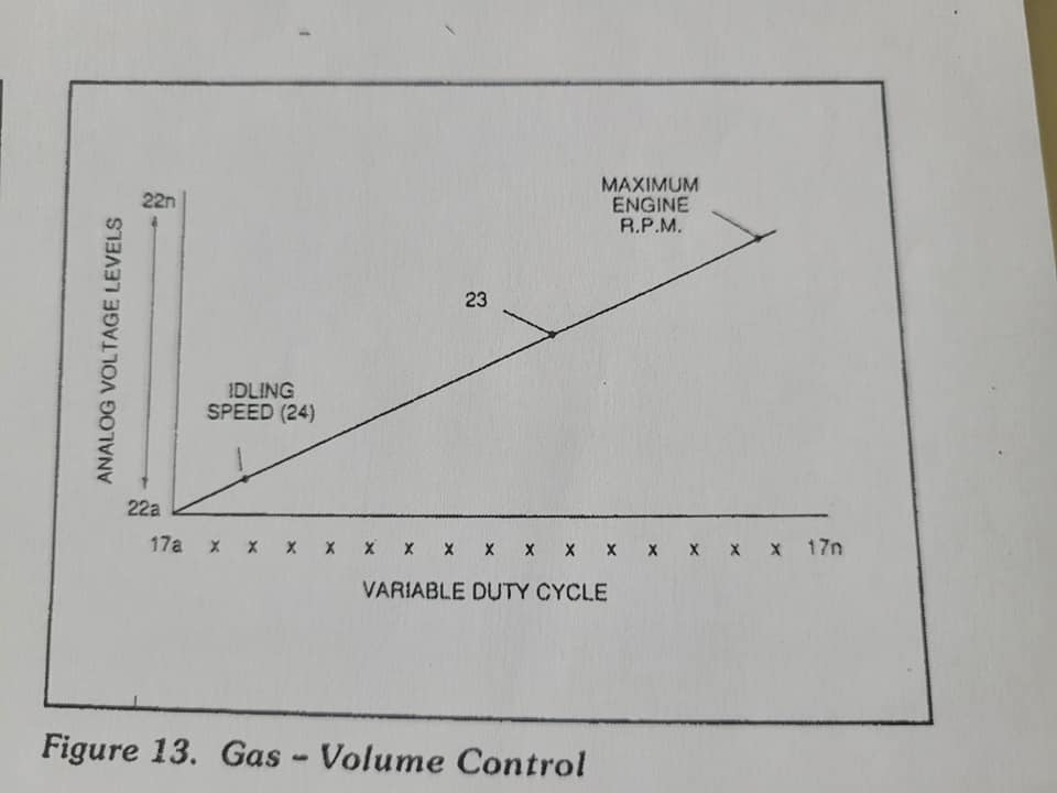
The generated digital signal (19) being electrically transmitted from accelerated control circuit (30) of Figure (4) is, now,electronically detected, translated, and converted into a analog voltage signal (22) which is continuously proportionate to Input signal (19) by ana- log voltage Generator Circuit (40) of Figure (4). The newly formed analog signal (22) of Figure (13) is a voltage level signal that varies continuously in both time and amplitude to produce a voltage level which is directly propor- tional to the physical change in pulse train (16a xxx 16n) of Figure (12). As pulse width (17ax) of signal (19) changes so does analog voltage level output (23) of Figure (13). Widening pulse width to stop-position (17a xxxxx 17n) of Figure (12) causes analog signal (22) to increase to higher voltages levels; whereas, analog voltage level (22) drops (become lower in value) in voltage level when pulse width decreases to start-position (17a). The resultant and varied voltage level (22a xx) varies smoothly over a continuous range of voltage valves (22a xxx 22n) rather than in discrete steps, as illustrated in linear graph (23) of Figure (13).
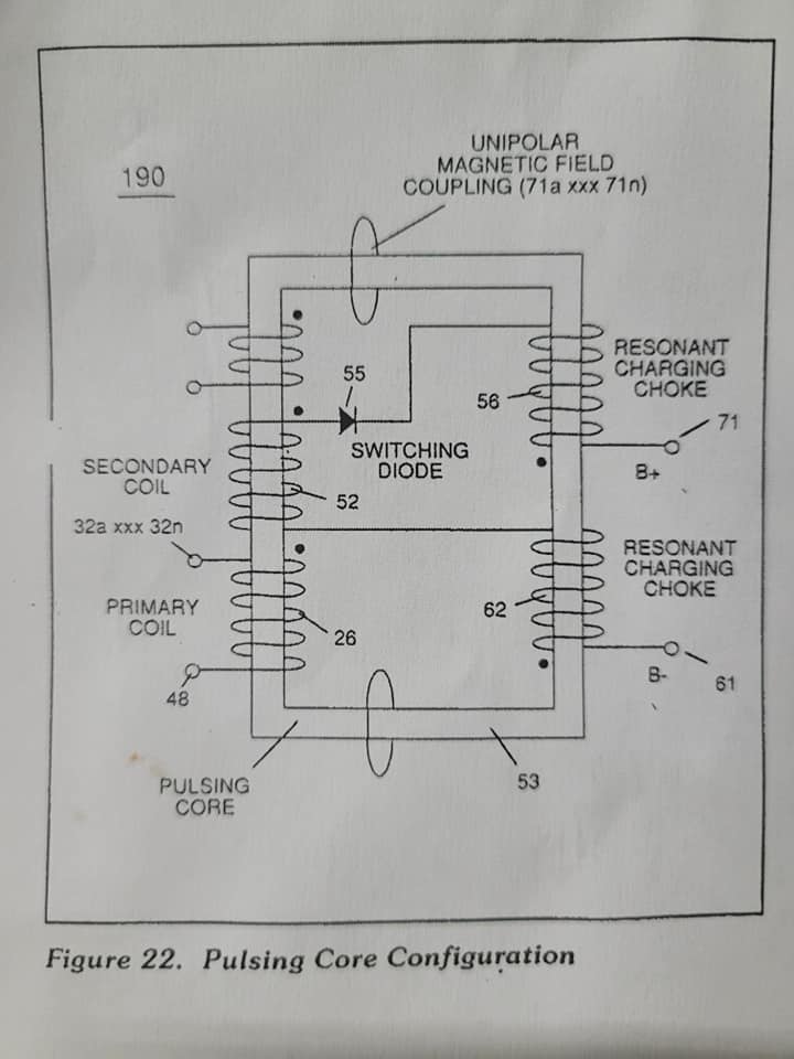
In terms of functionalability and purpose, analog circuit (40) of Figure (4) provides a variable (controlled) voltage output (23) in direct relationship to light-gate (9) displacement which, in turn, sets up and controls Resonant Action (160) of Figure (22) that pro- duces Fuel Gases on demand. Analog circuit (40) also calibrates both engine response). Idling speed (22ax) and maximum en- gine R.P.M. (22a xxx 22n) by adjusting and maintaining a predetermined or given low (24) and high voltage levels respectively, as further illustrated In Figure (13). Voltage valves or levels (22a xxx 22n) simply controls the ap- plied voltage potential across Reso- nant Cavity Assembly (120) of Figure (21) through voltage amplitude control circuit (50) of Figure (4) which is electri cally linked to primary coil (26) of Figure (20) of Voltage Intensifier Cir- cuit (60) of Figure (4).
Voltage Amplitude Control Circuit (50)
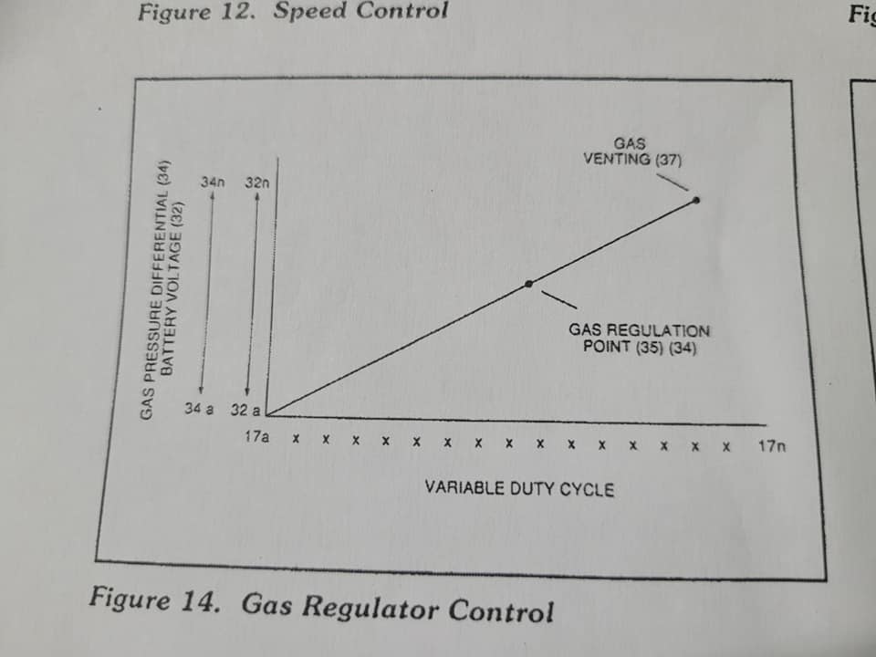
Voltage amplitude control circuit (50) of Figure performs several functions simultaneously. First, regulates car bat tery electrical voltage potential (32) of Figure (14) being applied to primary coll (26) of Figure (20), and secondly, regulates gas pressure of Fuel Cell(120) of Figure (21), as graphically depicted in Figure (14). Each regulatory stage(27) and (28) works separately and independent of each other but are electronically linked or coupled together to produce a common analog signal (32) having a predetermined voltage level (32a xx), as further shown in Figure (14)
Regulator stage (27) of circuit (50) converts battery voltage potential (29) of Figure (5) via electrical terminal (31) of Figure (4) as to Figure (5) Into an analog voltage signal (32) of Figure (14) which corresponds to but is electrically isolated (crossover voltage from two separate power supplies) from incoming gas volume signal (23) of Figure (13), as shown in Figure (4). Variable voltage range (32a xxx 32n) from one (1) up to twelve (12) volts (regulating battery voltage) is applied across primary coil (26) of Voltage Intensifier Circuit (60) of Figure (20). Second regulator stage (28) simply acts and function as a gas regulator (33) by preventing Fuel Gas production beyond a predetermined gas pressure level (34) of Figure (14) during Fuel Cell operations and, as such, maintains constant gas pressure to Fuel Injectors (36) of Figure () regardless of engine performance (R.P.M.
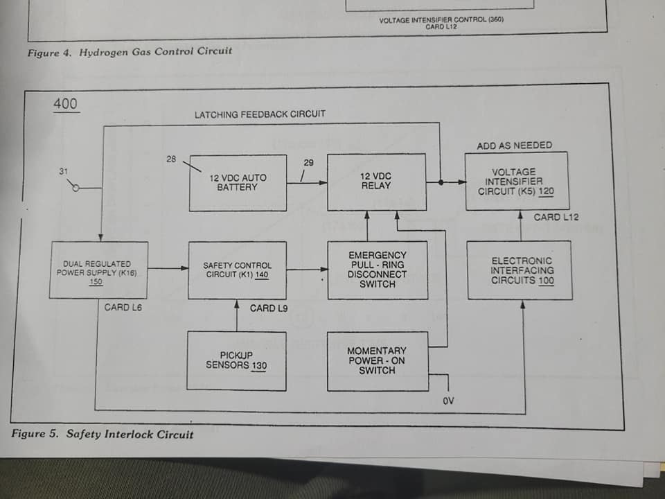
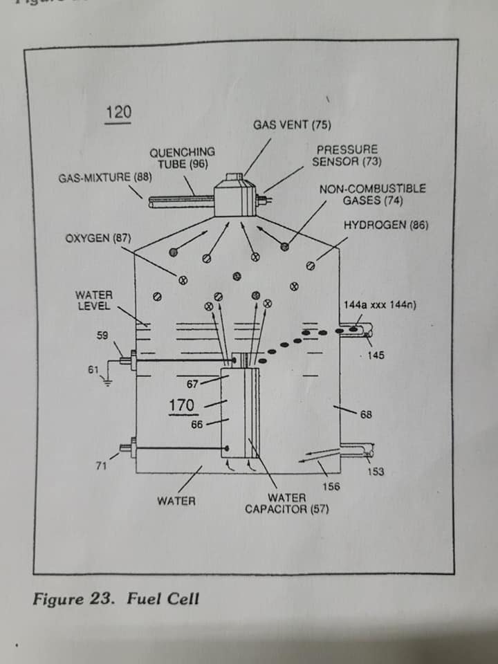
If for example, Fuel Gas production is greater than demand, then, analog signal (32) is reduced to proper voltage level (35) (voltage level directly deter mines gas pressure via Resonant Action) required to maintain gas pressure (34). Conversely, analog signal (32) is always allowed to exceed voltage level (35) during injection (36) of Figure () until gas-point (34) is reached. In cases where linear voltage (32) drops (descending value) below gaspoint (35) then gas regulator stage (28) Increases voltage amplitude (32a xxx 32n) (analog volt- age) to voltage point (35). If gas pres sure (34a xx) should exceed gas point (35) during injector offtime, gas pressure release valve (75) of Figure (23) (gas venting 37 of Figure 14) expels Fuel gases (88) until gas point (34) is either reached or a delay timing circuit activates Safety Control Circuit (14) of Figure (5) which, in ham, switches off or disconnects applied electrical power (28) to Fuel Cell electrical system (400) of Figure (5)
Gas logic circuit (310) of Figure (4) supplies logic function to Voltage amplitude control circuit (50) to maintain proper gas pressure to gas injector (36) of Figure ) by electronically monitoring achieved gas pressure via pressure sensor (73) of Figure (23) In terms of operability, Laser Accelerator Assembly (20) of Figure (4) is, now, attenuating battery voltage potential (32a xxx 32n) which is electrically connected to voltage Intensifier Circuit (60) of Figure (4).
Variable Pulse Frequency Generator (70)
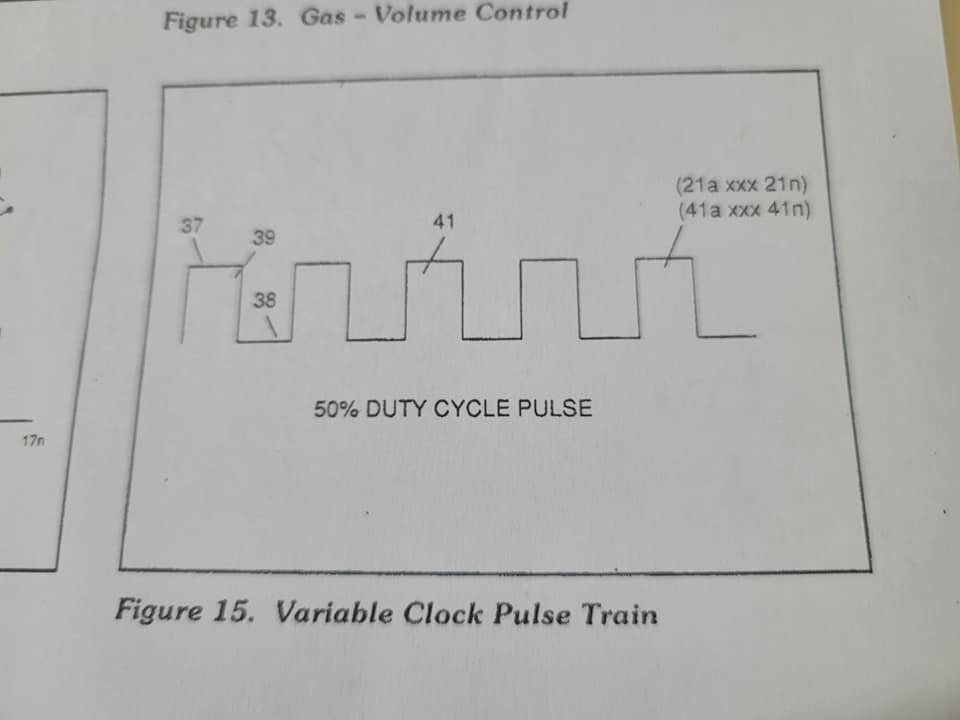
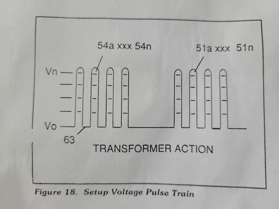
Circuit (70) of Figure (4) is a multi pulse-frequency generator which produces several clock pulses (simultaneously) having different pulse-frequency but maintaining a 50% duty cycle pulse (39) configuration, as illustrated in Figure (15). Pulse on-time (37) and pulse off-time (38) are equally dis- placed to form duty pulse (39) which is duplicated in succession to produce pulse train (41) of Figure (15). Increasing the number of duty pulses (39a xxxx 39n) up to pulse frequency range of 10Khz or above now forms clock signal (21) of Figure (4) which, in tum, per- forms the scanning function of Acceleration Control Circuit (30) of Figure (4) Circuit (70) also produces another Independent and separate clock signal (41a xxx 41n) which is electrically transmitted to and become incoming clock signal (42) for Gated Pulse Frequency Generator Circuit (80) of Fig. ure (4). In both cases, pulse frequency range of each clock signal (21) and (42) can be altered or changed (controlled Independent of each other) to obtain peak performance of Fuel Cell System (100) of Figure (4).
Gated Pulse Frequency Generator (80)
Gated Pulse Circuit (80) of Figure (4) switches "off" and "on" sections of Incoming clock signal (42) to form gated pulse (45) which is, in turn, duplicated in succession to produce gated pulse train (46a xoox 46n) of Figure (16). Together pulse train (44a xxxx 44n) and pulse off-time (43) forms gated pulse duty cycle (45). Pulse train (44a xxx 44n) is exactly the same as pulse train (41a xxxx 41n) and its established pulse frequency (number of pulse cycles per unit of time) changes uniformly when pulse generator (70) of Figure (4) is calibrated and adjusted for system operations.
Newly formed gated duty pulse (45) is proportional to the physical change in pulse train (44 xxx 44n) when circuit (80) is adjusted for calibration purposes. Pulse train (440 xxx 44n) be- comes widen while pulse off-time width (43) becomes smaller, simultaneously Conversely, opposite pulse shaping occurs when circuit (80) of Figure (4) is calibrated in reverse order.
Cell Driver Circuit (90)
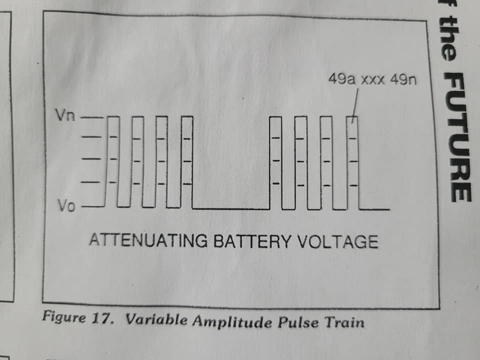
In either case, the resultant or varied pulse train (47a xxx 47n) (calibration of 448 xxx 44n) becomes incoming gated pulse signal (48) of Figure (4) to cell driver circuit (90) of Figure (4) which performs a switching function by switching "off" and "on" electric ground being applied to opposite side (48) of primary coil (26) of Figure (18). The resultant pulse wave form (49a xxxx. 49n) of Figure (17) superimposed onto primary coil (26) is exact duplicate of proportional pulse train (47a xxxx 47n). However, each pulse train (47) (49) are electrically isolated from each other. Only voltage cross-over from regulated power supply (150) of Figure (5) to battery supply (28) occurs, as illustrated in Figure (5).