
The Fermi Level Barrier
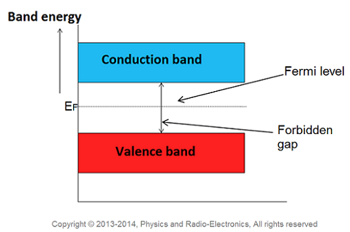 The Fermi level is a concept used in solid-state physics to describe the energy level at which electrons in a material have a 50% probability of being occupied. In the case of natural water and a 304L stainless steel electrode, the behavior of the Fermi level is important in understanding the electrochemical reactions that occur at the electrode-water interface.
Natural water, such as that found in lakes, rivers, and oceans, is a complex mixture of dissolved gases, ions, and organic compounds. These components can interact with the electrons in the water and affect the position of the Fermi level. The Fermi level of natural water is generally close to the energy level of the water's highest occupied molecular orbital (HOMO), which is the energy level of the highest occupied electrons in the water molecule.
304L stainless steel is a commonly used material for electrodes in electrochemical applications due to its excellent corrosion resistance and durability. The Fermi level of the metal can be affected by several factors, including the presence of impurities, defects, or surface treatments. In the absence of any external influences, the Fermi level of 304L stainless steel is typically located within the energy band gap of the material.
When a 304L stainless steel electrode is submerged in natural water, electrochemical reactions can occur at the electrode-water interface. These reactions involve the transfer of electrons between the electrode and the water, which can cause changes in the position of the Fermi level. If the electrode is more electronegative than the water, electrons will flow from the water to the electrode, causing the Fermi level of the water to decrease and the Fermi level of the electrode to increase. This can result in the formation of an electric double layer at the electrode-water interface, which can affect the behavior of ions and molecules in the water.
 The behavior of the Fermi level of natural water and a 304L stainless steel electrode is important in many electrochemical applications, including corrosion prevention, electroplating, and water treatment.
Understanding the electrochemical reactions that occur at the electrode-water interface can help to optimize these processes and improve their efficiency and effectiveness.
The position of the Fermi level can be affected by several factors, including the composition of the water, the surface condition of the electrode, and the electrochemical reactions that occur at the electrode-water interface. By understanding these factors, researchers and engineers can develop new and improved methods for electrochemical applications.
See Stephen Meyer's Radio Interviews for his unique perspective on the birth of the Schottkey diode, the behavior of the P-metal junction and how natural water introduces a doping effect on the SS 304L capacitor plate.
"Don't ask, what the metal electrode introduces to the water. Ask, what the water introduces to the metal electrode."
~ Stephen Meyer
The Schottky diode is a semiconductor device that has revolutionized electronics since its discovery in the early 20th century. It is named after the German physicist Walter H. Schottky who first observed the phenomenon of rectification in metal-semiconductor junctions in 1938. Schottky diodes are used in a wide range of electronic applications, from power conversion to radio frequency signal detection.
The basic principle behind the Schottky diode is the manipulation of the Fermi level of a semiconductor by the introduction of a metal layer. When a metal is deposited on a semiconductor material, it forms a junction that allows current to flow in only one direction. The metal-semiconductor junction behaves like a diode, allowing current to flow in only one direction, from the metal to the semiconductor.
The Schottky diode is different from a conventional p-n junction diode in that it has a metal-semiconductor junction, rather than a p-type and n-type semiconductor junction. The metal layer in the Schottky diode is typically made of a noble metal such as gold, platinum, or tungsten. The semiconductor material can be either p-type or n-type. The metal layer is deposited onto the semiconductor material through a process known as sputtering.
Schottky diodes have several advantages over p-n junction diodes. They have a lower forward voltage drop, faster switching speed, and lower reverse recovery time. These properties make them ideal for high-frequency applications such as radio frequency detection and power conversion.
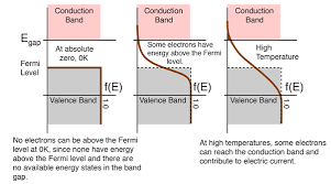
Experiments with P-metal and N-metal junctions have shown that doping can create either a resistive-like connection or a diode-like connection. Doping is the process of introducing impurities into a semiconductor material to alter its electrical properties. In p-type semiconductors, the doping introduces acceptor impurities, which create holes in the valence band. In n-type semiconductors, the doping introduces donor impurities, which create electrons in the conduction band.
By doping the semiconductor material, the Fermi level can be shifted, creating either a resistive-like connection or a diode-like connection. In a resistive-like connection, the Fermi level is near the middle of the bandgap, and the current flows in both directions. In a diode-like connection, the Fermi level is closer to the conduction or valence band, depending on the type of semiconductor material, and the current flows in only one direction.
The discovery of the Schottky diode and experiments with P-metal and N-metal junctions have greatly contributed to the development of modern electronics. Schottky diodes have found wide applications in areas such as power conversion, radio frequency detection, and digital electronics. The ability to manipulate the Fermi level of semiconductor materials through doping has enabled the development of advanced semiconductor devices such as transistors, integrated circuits, and light-emitting diodes.