(9)
Bypass Coil
Also written coil · Circuit Stage · interfacing circuit · coil winding
Where it is first named
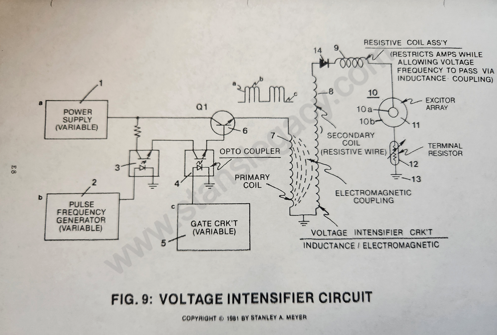
Purpose: To restrict amp flow while allowing voltage potential to pass through said bypass coil (9 of Figure 9) via electromagnetic induction coupling.
How it is written
- (9) 10×
- (8 as to 9) 1×
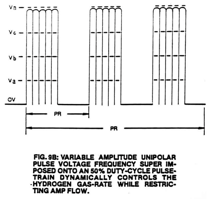
- (9 of Figure 9) 1× with Figure (9) Variable Amplitude Unipolar Pulse Voltage Frequency Super Im- Posed Onto An 50
Drawings 2
-
Circuit Stage: (7) (8), (14), (9), (10) as to (11), (10B), (12) and (13). · Voltage Attenuation Circuit
-
Purpose: To interface said pulsing circuit (Figure 9) with another type of power supply. · Voltage Attenuation Circuit
Where it is named · 12
Voltage Attenuation Circuit 12×
-
Purpose: To restrict amp flow while allowing voltage potential to pass through said bypass coil (9 of Figure 9) via electromagnetic induction coupling.
-
bypass coil (9)
As pulse voltage potential is developed across said secondary coil (8) leads, said developed voltage pulses are now allowed to pass through and beyond said bypass coil (9) by way of electromagnetic inductance.
-
coil (9)
Inductance coupling occurs when said voltage pulses generate an oscillating magnetic field around said bypass coil (9). The incoming voltage pulse creates a magnetic field that passes through said coil (9) windings.
-
coil (9)
Once the applied incoming voltage pulse is terminated, as herein described, the magnetic field now collapses, allowing said collapsing magnetic field to pass through said coil (9) once again during said voltage off-time.
-
coil winding (9)
Amp restriction occurs since said coil winding (9) is composed of resistive wire (sixth-stage to amp restriction).
-
bypass coil (9)
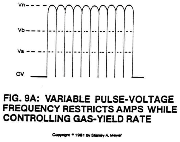
The pulse voltage waveform (mirror imaged of Figure 9B) developed at said bypass coil (9) output lead is now transferred to stainless steel plates (excitor array) submerged in natural water.
-
bypass coil (9)
Purpose: To provide ohmic balance between said bypass coil (9) and said ground terminal (13) to help eliminate electron deflection within said power circuit during gas production.
-
interfacing circuit (8 as to 9)
Terminal resistor (12 of Figure 9) is affixed to said excitor-array (10) on ground side (see Figure 9 again) to prevent counter electron deflection or movement within said interfacing circuit (8 as to 9).
-
bypass coil (9)
Said terminal resistor (12) is composed of resistive wire wrapped in a coil configuration, taking the shape of said bypass coil (9).
-
bypass coil (9)
Said bypass coil (9) and said terminal resistor (12) are the same in likeness.