Inductance Reactance (Rs - Cd - FL)
Inductance Reactance occurs when resistance (Rs), capacitance (Cd), and Inductance (FL) interacts together during D.C. Pulsing (49a xxx 49n), as schematically depicted in (690) of Figure (7-8).
|
(690) of Figure (7-8)
|
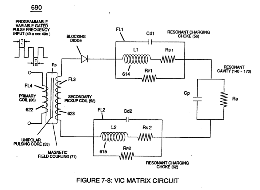
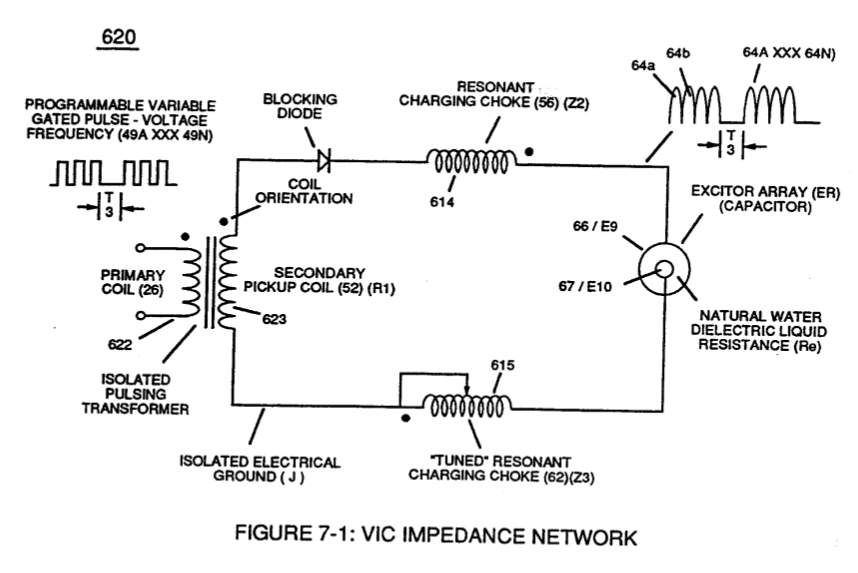
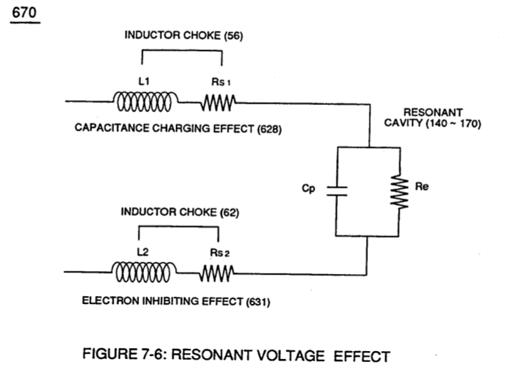
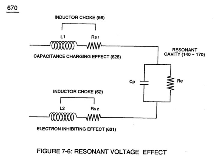
Inductance Reactance not only increases voltage across water-capacitor (ER) beyond applied Voltage Potential (626) of Figure (7-7) but, also, establishes "Impedance Field" (FL) across Inductors (L1-L2) of Figure (7-6) which acts and performs as Resonant Charging Chokes (614/615) of Figure (7-1) once placed on opposite side of capacitor (ER) forming Resonant voltage Effect Circuit (670) of Figure (7-6), as illustrated in (620) of Figure (7-1) as to (690) of Figure (7-8).
|
Voltage Potential (626) of Figure (7-7)
|
Inductors (L1-L2) of Figure (7-6) |
|
Resonant Charging Chokes (614/615) of Figure (7-1)
|
(670) of Figure (7-6)
|
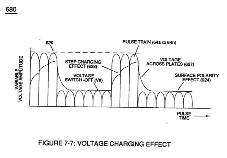
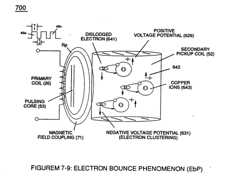
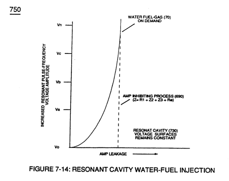 Both Inductors (LI/L2) are Bifilar wound in equal length to optimize the electromagnetic field strength (FL) in equal electromagnetic intensity (FL1 = FL2) to encourage and promote "Electron Bounce" phenomenon (700) of Figure (7-9) while adjusting (programmable pulse wave-form) input signal Pulse-Frequency (49a xx 49n) to "tune-in" to the "dielectric property" (Re) of water (85) causing amp flow to be reduce to a minimum value while allowing voltage potential (627) of Figure (7-7) to go toward infinity if the electronic components would allow it to happen, as graphically illustrated in (750) of Figure (7-14).
|
"Electron Bounce" phenomenon (700) of Figure (7-9)
|
(627) of Figure (7-7)
|
Inductance Field (L1-FL1) performs "Capacitance Charging Effect" (628);
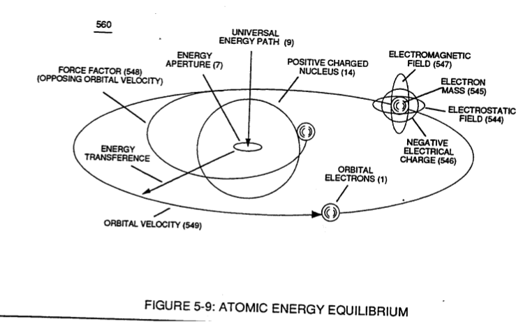
while, at the same time, Inductor Field (L2-FL2) restricts electron movement through VIC Impedance Network Circuit (620) of Figure (7-1) since Inductance Field (FL2) locks onto Electrons Magnetic Field (547) of Figure (5-9) to block the movement of electron flow toward Positive Voltage Potential (66)
|
(620) of Figure (7-1)
|
(547) of Figure (5-9)
(This reference was incorrect. 647 mentioned, but 547 was desired - CB) |
... thereby preventing and inhibiting electron-flow to pass through or arc-over capacitor water-gap (Cp) of Figure (7-8) such electron blocking action is herein called "Electron Inhibiting Effect" (631), as denoted in (670) of Figure (7-6) as to (750) of Figure (7-14).
|
(Cp) of Figure (7-8)
|
(670) of Figure (7-6)
|
|
(750) of Figure (7-14)
|
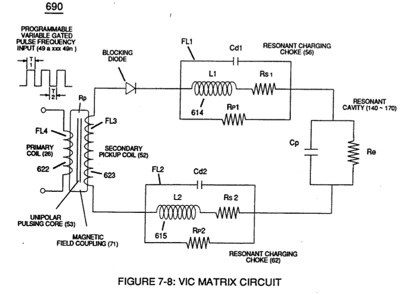
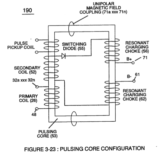
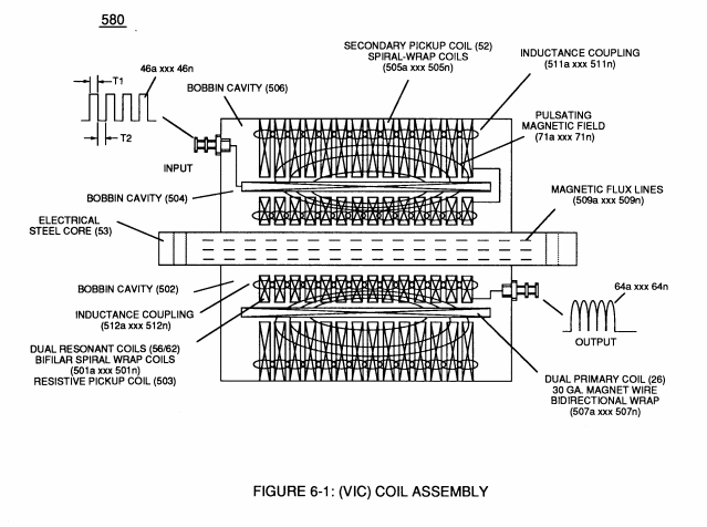
At elevated or higher amplitude voltage levels (xxx Ve xxx Vf xxx Vn), primary electromagnetic coupling field (Rp) of Figure (7-8) transmitted by way of Inductance Pulsing-Core (190) of Figure (3-23) as to VIC Coil Assembly (580) of Figure (6-1) enters into and passes through both Inductors (L1/L2) simultaneously and offers not only further electron-flow restriction (Rp1/Rp2) to both Inductor Chokes (56/62) but automatically increases voltage potential (xxx V g xxx Vh xxx Vn) of opposite voltage intensity of equal magnitude (66/67) across Resonant Cavity (140 -170)
|
(Rp) of Figure (7-8)
|
Inductance Pulsing-Core (190) of Figure (3-23)
|
|
VIC Coil Assembly (580) of Figure (6-1)
|
... overcoming any potential loss of pulse signal due to resistive interaction (Rsl/Rs2) of either or both Inductor Cores (L1/L2) wire-material to the formation of Inductance Fields (FL1/FL2) during reoccurring pulse on-time (T1a xxx T1n).
Electron Inhibiting Effect (631) in direct relationship to Voltage Enhancement Effect (528) is accomplished since stainless steel 430F/FR wire-material is "Electromagnetic Inductive" to incoming electromagnetic flux-lines (71a xxx 71n) (Rp) without (s/s) inductor-wire-coil (L1/L2) becoming permanently magnetized
... paralleling and performing the same electromagnetic characteristic of copper wire when it comes to magnetic field reformation (Rp - Rp 1 - Rp2) of Figure (7-8), as further illustrated in electromagnetic coupling fields (71 - 511 - 512) of Figure (6-1) that encourages, brings-on, and perform Voltage Inducement Process (580) of Figure (6-1) as to (620) of Figure (7-1) without amp "influxing" (inhibiting amp flow) between Positive Voltage Potential (66) and Negative Voltage Potential (67) electrically applied across Resonant Cavities (140 -170).
|
Figure (7-8)
|
Figure (6-1)
|
(620) of Figure (7-1)