
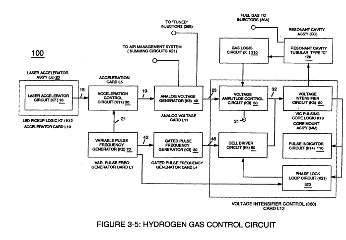
Acceleration Control Circuit (30)
Moving light-gate (9) of figure (3-9) in direct relationship to the physical placement of optical circuits (8a xxx 8n), sets up a time variable (14a xxx 14n) of Figure (3-7) from optical circuits (8x) to another optical circuit (8xx) and/ or (8xxx) or to (8n) since the triggered low logic state (12) of Figure (3-7) and (3-8) moves in direct relationship to the displaced light-gate (9), as
illustrated in Figure (3-12).
|
Figure (3-7)
|
Figure (3-8)
|
|
Figure (3-9)
|
Figure (3-12)
|
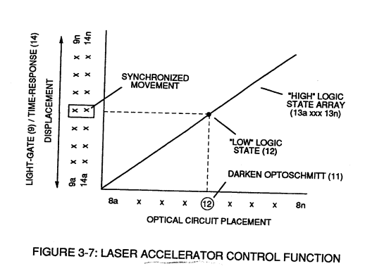
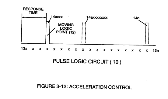
Deflecting (moving) the light-gate (9) to position (8n) takes longer in response-time (14n) than deflecting the light-gate to position (8x) and/or (8xx) or (8xxxx).
This variable response-time (14axx ... 12 ... xxI4n) or signal output (15) of Figure (3-5) is, now, electrically transmitted to Acceleration Control Circuit (30) of Figure (3-5) since Laser Accelerator Assembly (20) of figure (3-10) converts mechanical displacement (9a xxx 9n) to electrical time-response (14a xxx 14n) of Figure (3-7) by linearly moving (forward and/or reverse direction) "low" logic state signal (12) in a array of "high" logic state output signals (13a xxx 13n), as further illustrated in Figure (3-8) and Figure (3-12).
|
Figure (3-7)
|
Figure (3-5)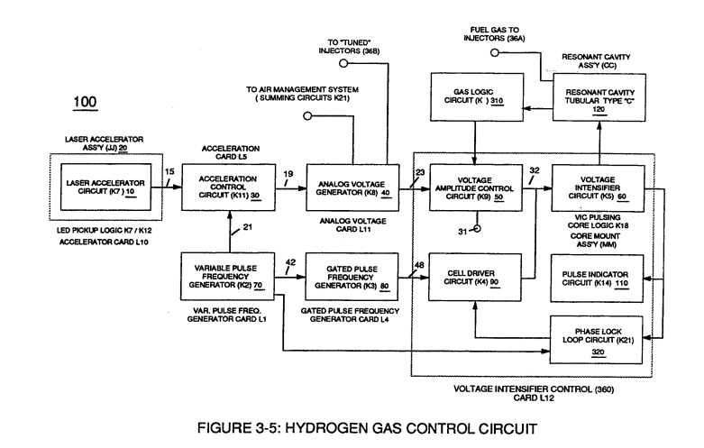 |
|
Figure (3-8)
|
Figure (3-12)
|
In some cases reverse signal-logic (12a xxx ... 13 ... xxx 12n) is applicable by using SDP 8601 Optoschmitt which switches logic state from Quiescent state ("low" to "high" logic state) when de-energized.
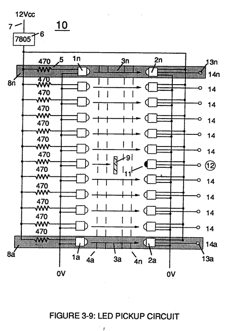 Since Led Pickup Circuit (10) of Figure (3-9) operates up to 100 kHz range or above, electrical sensitivity of Opto-circuit (8) provides a instantaneous response to Driver's acceleration, de-acceleration, or cruise control demands.
As signal output (15) of figure (4) (14a xxx ... 12 ... xx14n) is being received by acceleration control circuit (30) of Figure (3-5) as to Figure (3-12), circuit (30) converts incoming time-response signal (14a xxx ... 12 ... xx14n) into a variable time-base unipolar pulse (16), as shown in Figure (3-8).
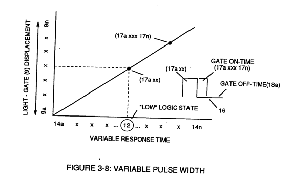
Circuit (30) electronically and automatically scans output signal-array (14axxx ... 12 ... xx14n) (15) until circuit (30) locates, momentarily registers, and translates response-time (14a xxx ... 12) into a variable unipolar pulse (17/18) of Figure (3-8).
The sweeping action of the scanning circuit (30) always starts from position (9a) and moves point (8ax) to point (8axxx) of Figure (3-9) (3-12) until logic-point (12) is detected.
Once logic signal (12) is detected, the sweeping action toggles and recycles back to start-position (9a).
This toggling (flip back) action electronically determines variable time-response (14a xxx) regardless of wherever logic point (12) is being momentarily displaced within circuit array (13a xxx 13n).
 Toggling action at full-scale deflection (13a xxx 13n) occurs in the range of (10) kHz or above and thus, allows instant response to driver's acceleration demands.
Toggling-time (scanning-time) is directly synchronized to light gate (9) displacement which, in turns, circuit (30) further sets up and establishes a given pulse shape (16) of Figure (3-8).
Circuit (30) continues to increase pulse width (17axxxx) of Figure (3-8) as the monitored (detected by < scanning) toggling-time (14a xxxx ... 12) increases when logic-point (12) moves farther away from start-position (9a) to stop-position (9n), as further shown in Figure (3-13) as to Figure (3-12).
Pulse width (17a xxx 17n) diminishes when logic-point (12) reverses direction to start .. position (9a).
Figure (3-12)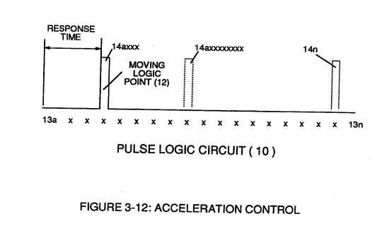 |
Figure (3-13) |
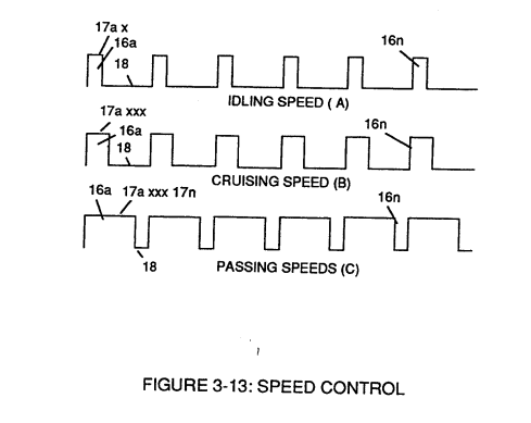
Finally, circuit (30) reproduces the variable controlled pulse-shape (16) in a continuous repetitive manner (16a xxx 16n) of Figure (3-13) and electrically transmits the resultant pulse-train signal (19) to Analog Voltage Circuit (40), as shown in Figure (3-5).
|
Figure (3-13)
|
Analog Voltage Circuit (40), as shown in Figure (3-5) |
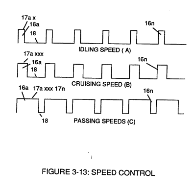
In retrospect to engine performance (gas pedal attenuation) (21) of Figure (3-10), a wider pulse width (17a xxx) of Figure (3-13C) increases (accelerates) engine R.P.M.;
whereas, smaller pulse-width (17ax) reduces (de-accelerates) engine R.P.M .. Cruising speed (3-13B) of Figure (3-13) is simply accomplished when pulse width remains constant.
Incoming clock pulse (21a xxx 21n) of Figure (3-16) originating from Pulse Frequency Generator (70) of
|
Figure (3-16)
|
Figure (3-5)
|
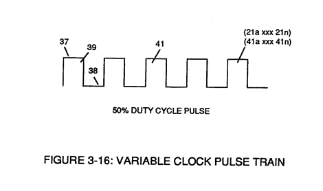
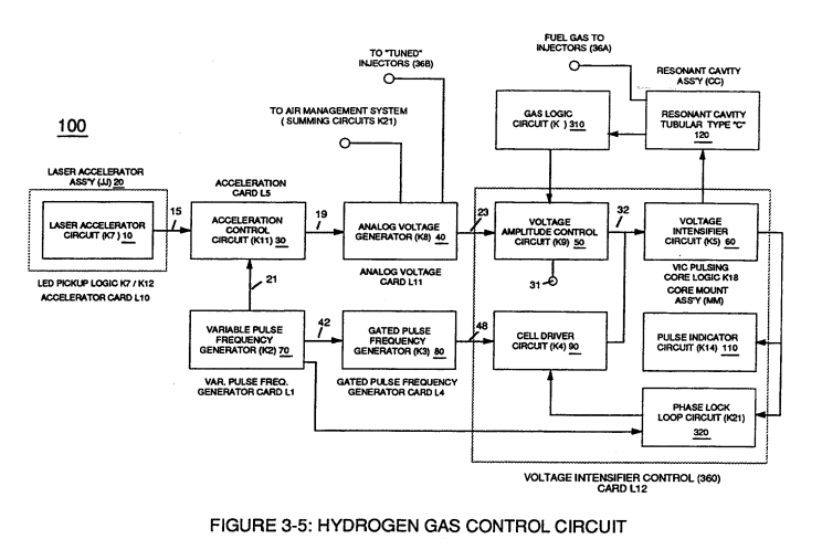
sets up the scan-rate (toggling) by which signal input (15) of Figure (3-5) is electronically scanned by circuit (30).
The resultant clock pulse (21) of Figure (3-16) as to Figure (3-5) is always adjusted to exceed driver's response time to allow for instant acceleration control.