
Inductance (FL)
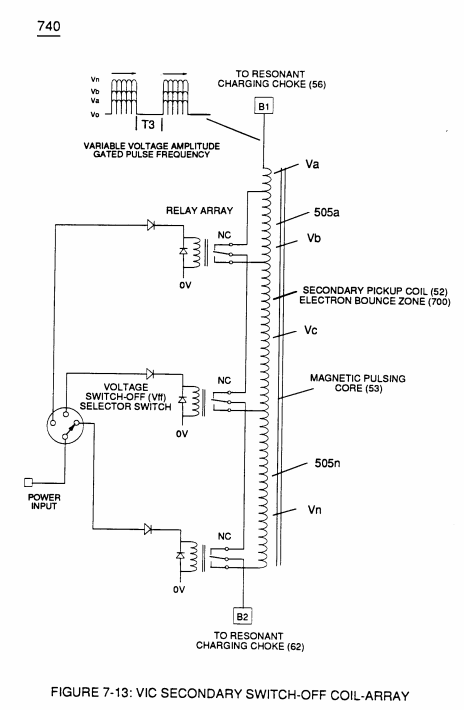
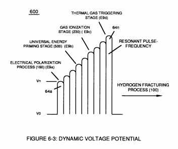
Component Interaction promotes Component Reactance during D.C. pulsing operations while allowing variable voltage amplitude (Vo - Va -Vb - Vn) of Figure (7-13) to be attenuated independently of Voltage Pulse frequency (49a xxx 49n), as so illustrated in (600) of Figure (6-3).
|
Figure (7-13)
|
(600) of Figure (6-3)
|
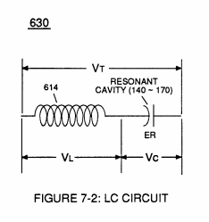
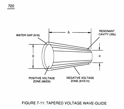
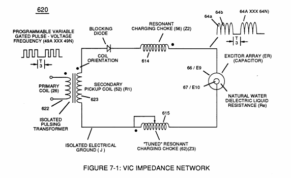
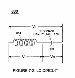
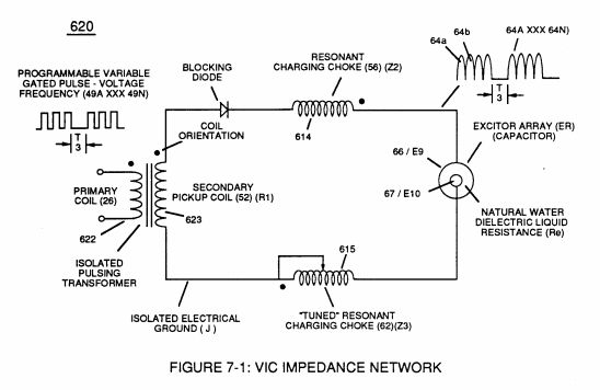
Resonant Charging Circuit (630) of Figure (7-2) being an LC Circuit is fanned when Inductor (614) of Figure (7-1) is electrically linked to Taper Capacitor (720) of Figure (7-11) in series arrangement.
|
(630) of Figure (7-2)
|
(614) of Figure (7-1)
|
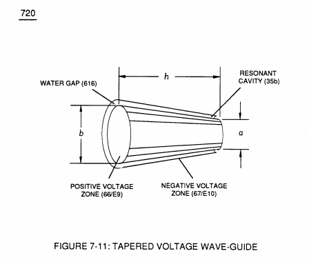
(720) of Figure (7-11)
|
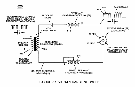
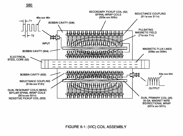
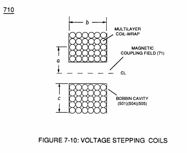
Inductor (614) is an insulated wire wound in a spiral pathway around Bobbin Cavity (580) of Figure (6-1) to form Voltage Stepping Coil (710) of Figure (7-10) as to (580) of Figure (6-1).
|
(580) of Figure (6-1)
|
(710) of Figure (7-10)
|
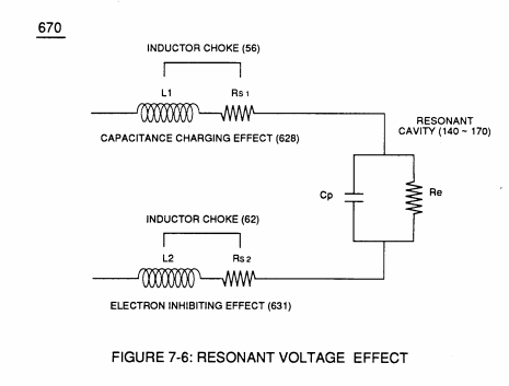
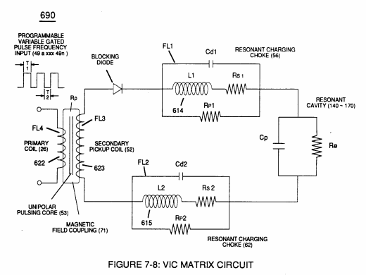
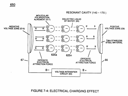
Capacitor (E9/E10) of figure (6-2) as to (720) of Figure (7-11) is formed when outer tapered surface (66) and inner tapered surface (67) forms Water-Gap (616) of Figure (7-11) as to Figure (590) of Figure (6-2) having placed there between Dielectric Water Bath (85/Re), as schematically illustrated in matrix outline in (670) of Figure (7-6) as to (690) of Figure (7-8) and further detailed in Electrical Charging Effect (650) of Figure (7-4).
|
(E9/E10 & 590) of figure (6-2)
|
(720, 616) of Figure (7-11)
|
(650) of Figure (7-4)
|
|
(670) of Figure (7-6)
|
|
(690) of Figure (7-8)
|

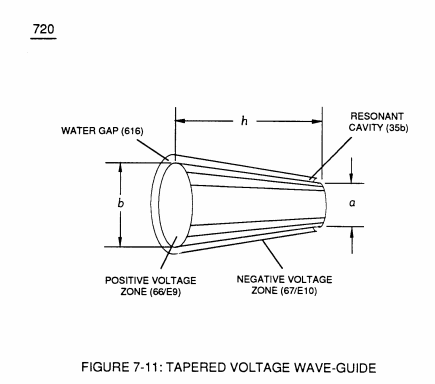

Component Reactance to D.C. pulsing transforms Inductor (614) of Figure (7-1) / Capacitor (E9/E10) of Figure (7-11) LC circuit of Figure (7-2) into an Resonant Charging Choke (614) which steps up an unipolar oscillation of an given charging frequency with the effective capacitance of a pulse-forming network (64a xxx 64n) of Figure (7-1) as to (600) of Figure (6-3) in order to charge Voltage Zones (E9/E10) to a higher potential beyond applied voltage input
|
Inductor (614) of Figure (7-1)
|
Capacitor (E9/E10) of Figure (7-11)
|
LC circuit of Figure (7-2)
|
|
|
(600) of Figure (6-3)
|
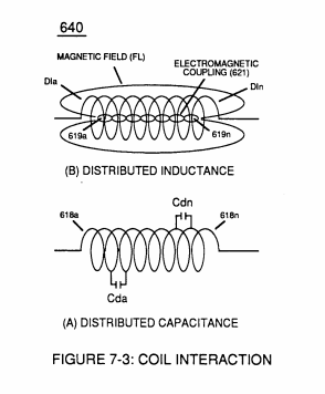
... interacting Distributed Capacitance (Cda xxx Cdn) and Distributed Inductance (D1a xxx D1n) of Figure (7-3) of Inductor Coil (614) of (7-1) with "Electrical Charging Effect" brought on by the dielectric value of water bath (85/Re), as pictorially illustrated in (650) of Figure (7-4).
(650) of Figure (7-4)
|
Figure (7-3)
|
(614) of (7-1)
|
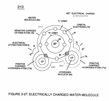
The established Dielectric Value of Water (85) being 78.54 ohms since the electron "L" orbit of the water molecule (210) of Figure (3-27) occupies the maximum allowable number of eight electrons when covalent linkup of 'unlike oxygen atom (76) and hydrogen atoms (77a/b) occurs' stabilizing Water molecule (85) into existence ... thereby, maintaining molecular stability of water by opposing the exchange of electrons from an external electron source (amp inducing circuit) beyond molecular Structure (85).
|
(210) of Figure (3-27)
|
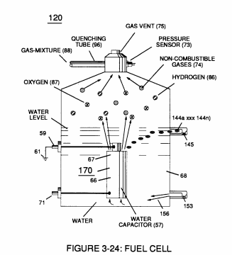
Electron interaction (movement of electrons through the liquid medium of water) is further inhibited since natural water contaminates (144a xxx 144n) of Figure (3-24) is normally less than 20 ppm.
Figure (3-24)
|
(760) of Figure (7-15)
|
(750) of Figure (7-14)
|
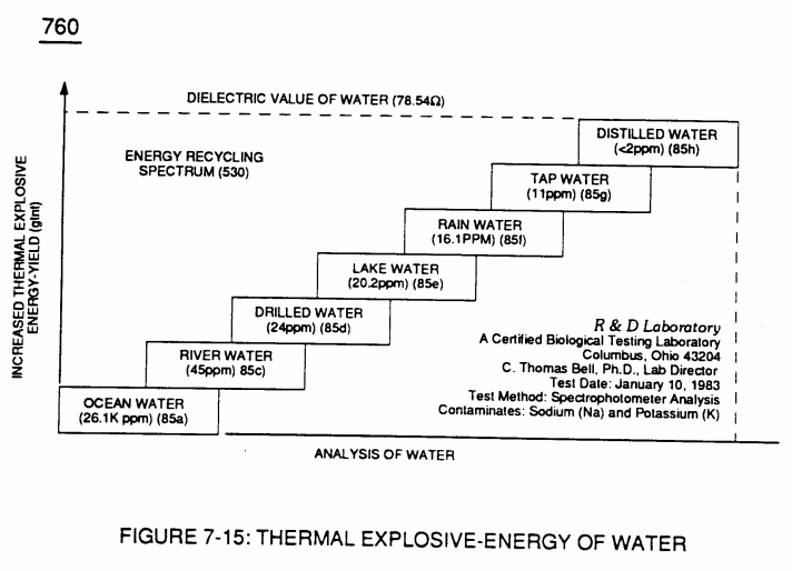
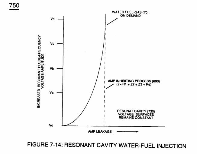
... distilled water, of course, is generally lab-tested 1ppm or less, as illustrated in (760) of Figure (7-15) as to (750) of Figure (7-14).