
Propagating Electrical Stress
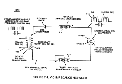
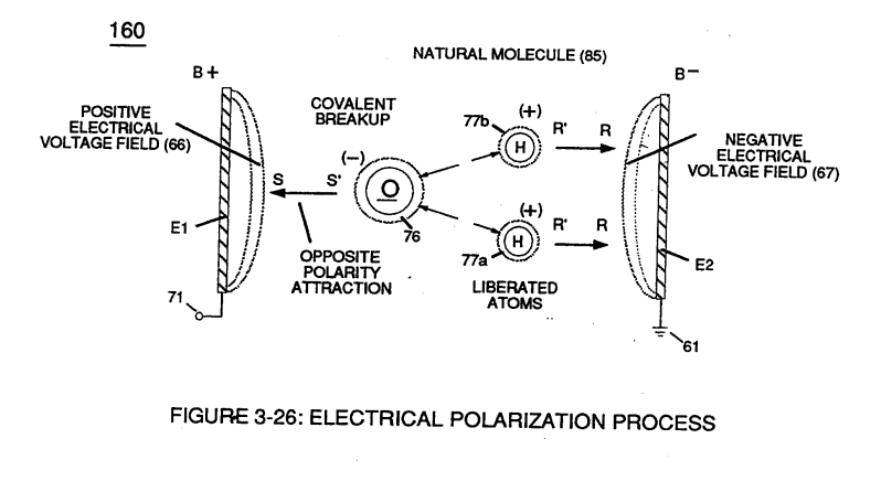
As in reference to WFC Patent Validation Report dated January 14, 1983 as per WFC Test-Results "Mode of Operability" of using "Voltage Potential" to "Dissociates the Water Molecule" by way of the "Electrical Polarization Process" (160) of Figure (3-26) as so specified under U.S. Patent Law (35 USC 101) demonstrate operability, the applied Pulse-Voltage Frequency is adjusted to tune-in to the dielectric properties of water by the use of WFC "Amp Inhibiting Circuit" (970) of Figure (10-1), as further illustrated in WFC Tech-Brief titled "The Birth of New Technology"
... U.S. Patent Memos 420 - 428, including "Table of Tabulation"
(Appendix A) as to "Glossary of Application Notes" (Appendix B).
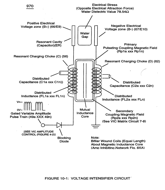
The Amp Inhibiting Circuit (970) of Figure (10-1) as to (690) of Figure (7-8) is composed of two copper wires "Bifilar" wound (wrapped) about a magnetic induction core to allow amp restriction (minimizing current leakage) while encouraging "Voltage Potential"(Va xxx Vn) across the water molecule to perform WFC "Electrical Polarization Process", as so illustrated in Figure (7-1) WFC memo (426) titled VIC Matrix Circuit.
|
Amp Inhibiting Circuit (970) of Figure (10-1)
|
(690) of Figure (7-8)
|
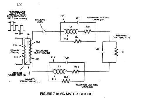
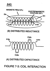
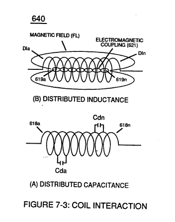
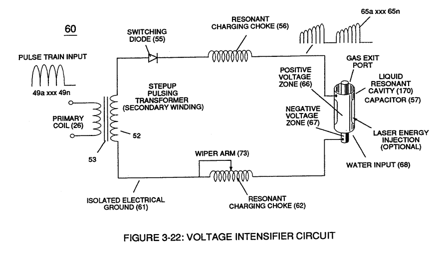
The energized "Resonant Charging Choke" (56) of Figure (7-1) as to Figure (10-1) by way of input voltage-pulses (49a xxx 49n) creates an electromagnetic coupling field (Rp1) of Figure (7-8) due to its self-inductance (640) of Figure 7-3B) crosses over and passes through electrically ground connected Resonant Charging Choke (62), as so illustrated in Figure (10-1)
|
"Resonant Charging Choke" (56) of Figure (7-1)
|
self-inductance (640) of Figure 7-3B)
|
... causing amp flow restriction during each pulsing-cycle since electrons exhibit electromagnetic characteristic
... forming "Mutual Inductance Fields" (Rp1/Rp2) once secondary coil (62) is electromagnetically energized by primary coil (56) and vice versa
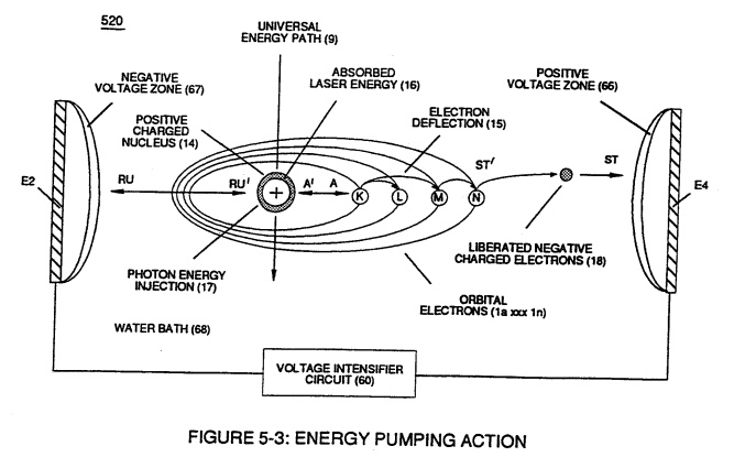
... thereby, preventing amp "in-fluxing" (discouraging electron arc over) across Dielectric Capacitor Gap (ER)(66/67) while Electrical Stress (ST-ST' - RU-RU') of Opposite Voltage Polarity (B+/B-) brings on Energy Priming Stage (520) of Figure (5-3) which is refer to, herein, as "Voltage Tickling of State Space."
|
Energy Priming Stage (520) of Figure (5-3)
|
The resultant Amp Inhibiting Circuit Figure (10-1) as to Figure (10-3 A/B) further allows amp restriction (minimizing current leakage) to be continued even if applied "Voltage Amplitude" is increased. The length and diameter size of the copper-wire spiral wrapped coil (56/62) of Figure (10-1) being paired together and electrically energized in conjunction with applied Voltage Pulse-Frequency determines how much "Amp Leakage" will occur across capacitor Gap (Cp) while "Voltage Pulse-Potential" (Va xxx Vn/49a xxx 49n) of "Opposite polarity" (B+/B-) is/are allowed to be applied across "Electrical Voltage Plates" (Voltage-Zones) (66/67).
|
Amp Inhibiting Circuit Figure (10-1)
|
Figure (10-3 A/B)
|
To reduce amp leakage still further, the copper wire of both Resonant Charging Chokes (56/62) can be replaced with a magnetically inductive stainless steel wire (430F/FR) having a resistive value (Ohms) to the flow of electrons while taking on the capacitance and inductance characteristic of a coil wire.
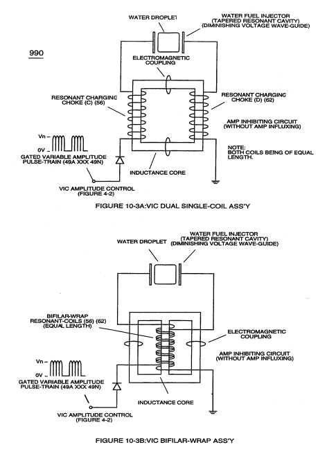
VIC Bifilar Wrap Coil-Assembly (10-3B) and VIC Dual Coil Wrap-Assembly (10-3A) both utilize either "E" & “I” and "U" Inductance Core configurations to concentrate Mutual Inductance Fields (Rpl/Rp2) in order to optimize Amp Inhibiting Process (750) of Figure (7-14).
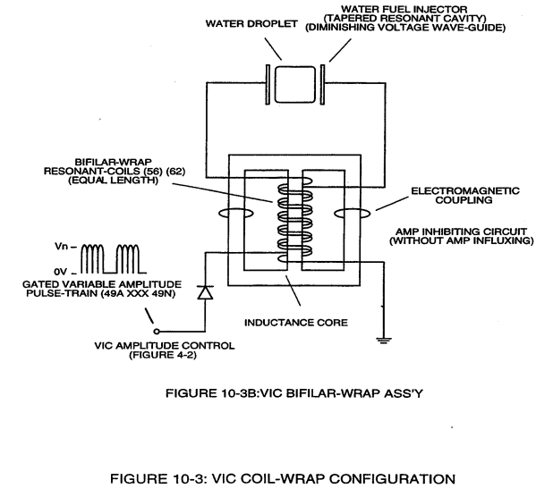 "E" “I” core shape (10-3B) is most preferable since amp spike surge is minimize during repetitive pulsing operations.
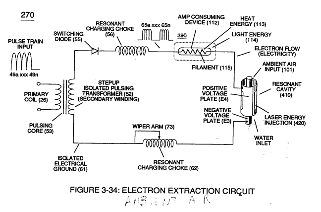
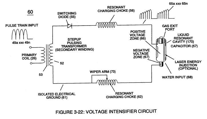
 Beyond amp restricting characteristic of said Amp Inhibiting Circuit (970) of Figure (10-1) as to Voltage Intensifier Circuit (60) of Figure (3-22), the spiral-wrapped coils (Resonant Charging Chokes 56/62) being paired together, also, causes voltage level enhancement beyond applied voltage input since the "Distributed Capacitance" (C1a xxx C1n - C2a xxx C2n) / "Distributed Inductance" (FL1a xxx FL1n - FL2a xxx FL2n) of said "bifilar" wrapped coils (Figure 7-3) as to (990) of Figure (10-3) encourages the compounding effect (increasing magnetic field-strength during each pulsing cycle) of electromagnetic field-strength (Rp1a xxx Rp1n - Rp2a xxx Rp2n) (mutual induction) when applied Pulse-Voltage frequency (49a xxx 49n) of Figure (3-34) passes through the positive energized Resonant Charging Choke (56).
|
Figure (3-34) |
Voltage Intensifier Circuit (60) of Figure (3-22)
|
|
"bifilar" wrapped coils (Figure 7-3)
|
(990) of Figure (10-3)
|
Furthermore, the paired coil-wires opposite voltage potential [positive electrical attraction force (B+) - negative electrical attraction force (B-)] [hereinafter called Electrical Stress (SS' - RR') as to (160) of Figure (3-26)] are always equal in electrical magnitude/intensity since the wire-lengths of each coil are the same.
|
(160) of Figure (3-26)
|
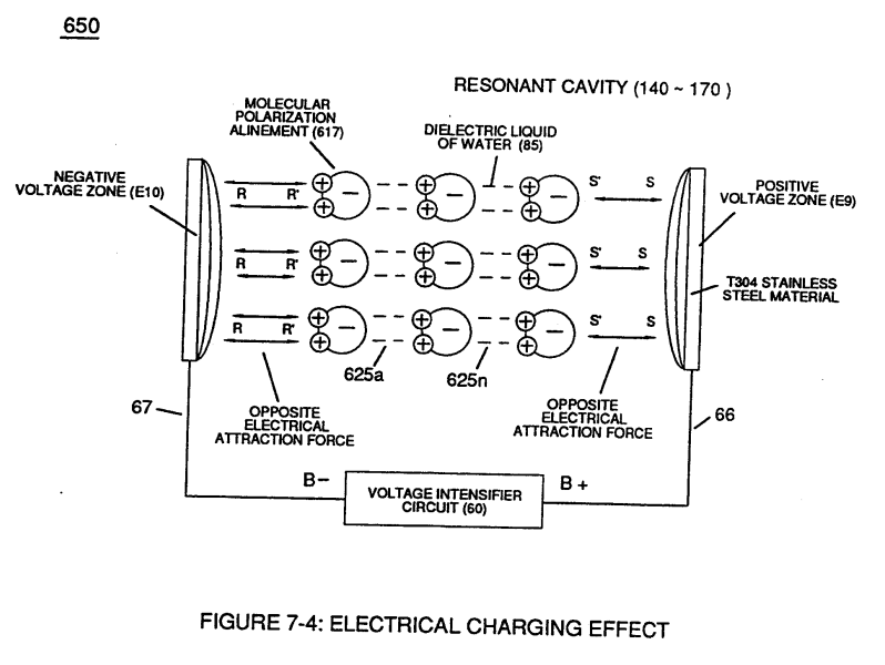
Pulse-Voltage repetition rate sets up the step-up charging effect Figure (1-3) since the "Resonant Cavity" (Cp) functions as a "Capacitor" (ER) due to the dielectric value of the liquid (or gases) which becomes an integral part of the VIC Circuit, as so illustrated in (650) of Figure (7-4).
The resultant voltage enhancement (Voltage Amplitude) can exceed 40 kilovolts to instantly convert water (droplets) into thermal explosive energy (gtnt) on demand, as so illustrated in Voltage Intensifier Circuit Diagram (970) of Figure (10-1).
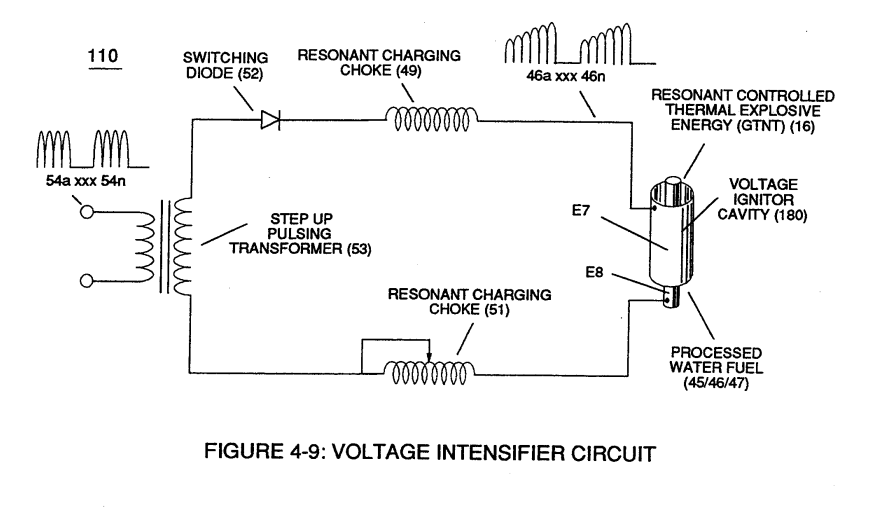
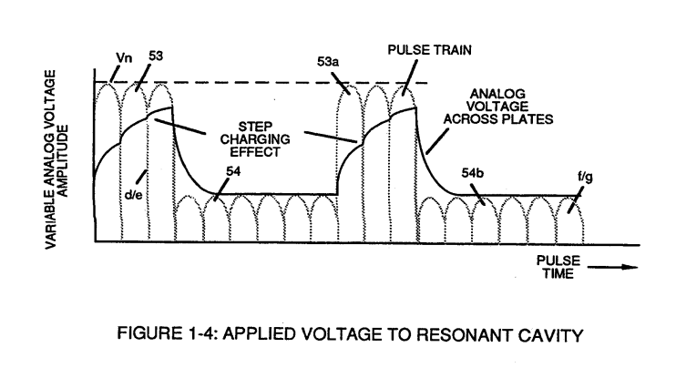
Blocking Diode (52) of Figure (4-9) as to Figure (1-1) allows unipolar pulse-wave to go more positive on each pulse-cycle since the Blocking Diode (52) prevents the Resonant Cavity (Cp) from discharging during pulse off-time, as so illustrated in Figure (1-4) as to (60) of Figure (3-22)
|
Blocking Diode (52) of Figure (4-9)
|
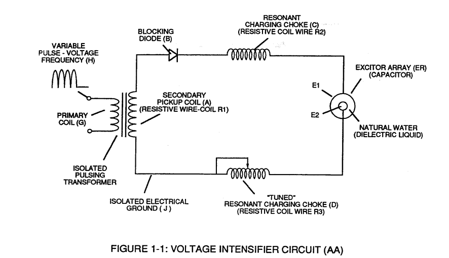
Figure (1-1)
|
|
Figure (1-4)
|
(60) of Figure (3-22)
|
... allowing the developed "Electrical Stress" (RU/RU' - ST/ST') of Figure (5-1/5-2) across Capacitor Gap (Cp) to go to the farthest point beyond the "State of Equilibrium"
|
Figure (5-1)
|
Figure (5-2)
|
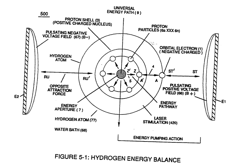
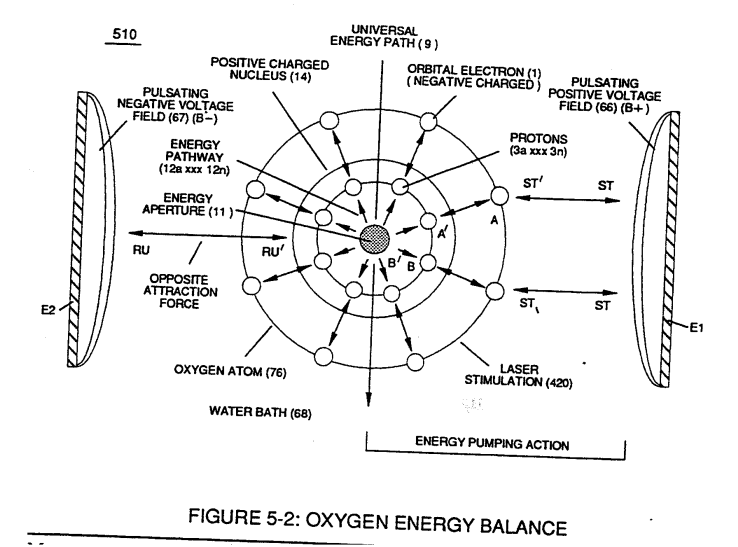
... see Atomic Energy Balance of Water (WFC memo 424), once again.
The programmable pulse-frequency (49a xxx 49n) of Figure (10-1) input is simply adjusted to tune-in to the dielectric property of the Water Molecule.
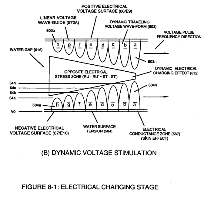
The resultant Dynamic Electrical Charging Effect (612) of Figure (8-1) acts as a progressive energy enhancer (Energy Priming Stage) (500) of Figure (5-1)
|
Dynamic Electrical Charging Effect (612) of Figure (8-1)
|
Energy Priming Stage (500) of Figure (5-1)
|
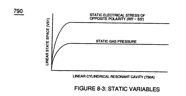
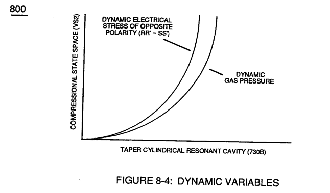
when Static State Space (790) of (8-3) is configured to Dynamic State Space (800) of Figure (8-4), as so illustrated in WFC memo (427) titled "Voltage Wave-Guide"
|
Static State Space (790) of (8-3)
|
Dynamic State Space (800) of Figure (8-4)
|
... whereby, the Voltage Wave-Guides forms Water Gap (Cp).