
Cell Driver Circuit (90)
In either case, the resultant or varied pulse train (47a xxx 47n) (calibration of 44a xxx 44n) becomes incoming gated pulse signal (48) of figure (3-5) to cell driver circuit (90) of Figure (3-5) which performs a switching function by switching "off' and "on" electric ground being applied to opposite side (48) of primary coil (26) of Figure (3-19).
|
Figure (3-18)
|
Figure (3-19)
|
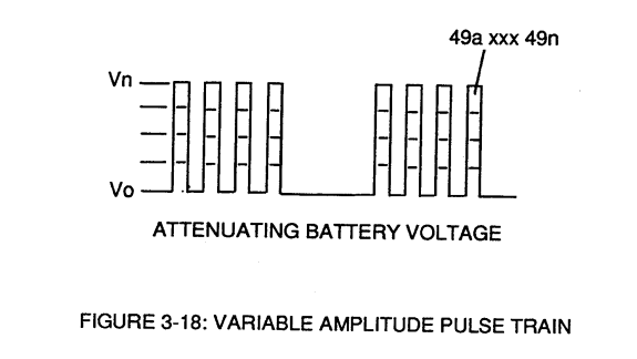
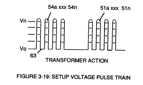
The resultant pulse wave form (49a xxx 49n) of Figure (3-18) superimposed onto primary coil (26) is exact duplicate of proportional pulse train (47a xxx 47n).
However, each pulse train (47) (49) are electrically isolated from each other.
Only voltage cross-over from regulated power supply (150) of Figure (3-6) to battery supply (28) occurs, as illustrated in Figure (3-6).
Figure (3-6)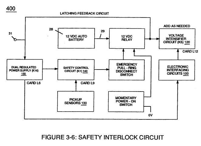 |
Figure (3-5)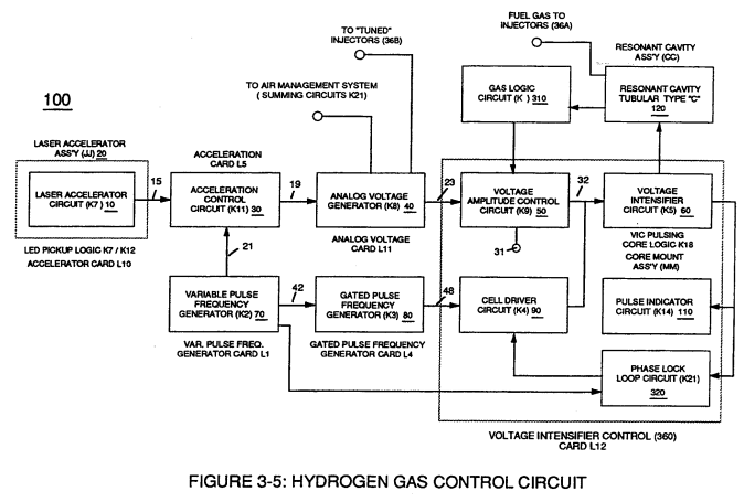 |